
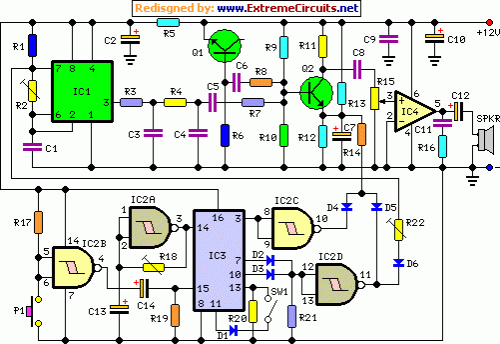
Monitor circuit diagram with over 555
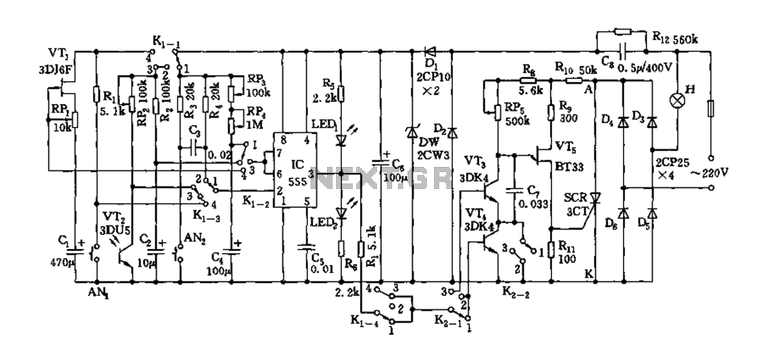
The 555 timer IC is a highly versatile component widely used in various electronic applications due to its ability to operate in different modes. The configuration of the circuit is dependent on the connections made to the external components, including resistors, capacitors, and switches. The K1 and K2 switches play a crucial role in determining the operational mode of the circuit.
In the first mode, when K1 and K2 are both set to position one, the circuit functions as a precise exposure timer. This mode allows for timing adjustments from 0 to 100 seconds, making it suitable for applications such as photography where specific exposure durations are required. The timing is controlled by the RC network formed by the resistors and capacitors connected to the timer.
In the second mode, with K1 and K2 in position two, the circuit's output at pin 3 is disconnected, which effectively isolates the dimming circuit. This allows for independent control of the light intensity by adjusting the variable resistor RP2. The configuration enables the user to determine the necessary exposure time for film by measuring the output voltage corresponding to the light intensity.
The third mode, activated by setting K1 to position three and K2 to position one, transforms the circuit into a light control switch. This configuration utilizes the variable resistor RP2 and transistor VT2 to adjust the trigger point of the timer IC, providing flexibility in light control applications.
Finally, in the fourth mode, the functionality of the delay can be toggled based on the position of switch K2. This allows for the implementation of a delayed activation feature, which can be useful in various timing applications where a specific delay is required before the circuit becomes active.
Overall, this circuit exemplifies the flexibility of the 555 timer IC, demonstrating its capability to function as a timer, dimmer, light control switch, and delay circuit through simple adjustments of external components and switches.Depending on the external circuit connection, 555 may be formed start delay, trigger delay, multi-harmonic oscillation mode and other working conditions, it is with some RC com ponents, switches and the like multi-purpose tester. By setting the control of the K1, K2 switch, the circuit can have exposure timing, dimming, delay and other functions. When the K1, K2 set to 1 position, it can be used as 0 to 100 second exposure timing circuit. When the K1, K2 are placed in the 2 position, IC 3 feet dimming circuit is broken K1-4, VT4 was K2-2 short front and rear circuit is independent state.
In this state, adjust the scale value on RP2, can be measured to know the exposure time required for the film. When K1 is set to 3 position, K2 is set to 1 for light control switch circuit, RP2 VT2 for adjusting the trigger end of the IC from the control point.
When K1 is set to 4, you need to select the location of the delay based on K2, the delay can be opened and closed function is activated.
Related Circuits
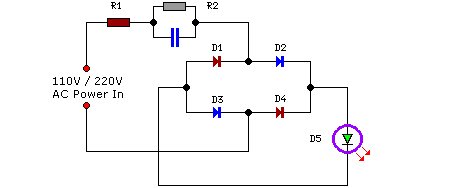
This is a straightforward and effective LED circuit that can be powered directly from an AC mains supply ranging from 100 volts to 230 volts. The circuit can serve as a mains power indicator or a night lamp. Resistors...
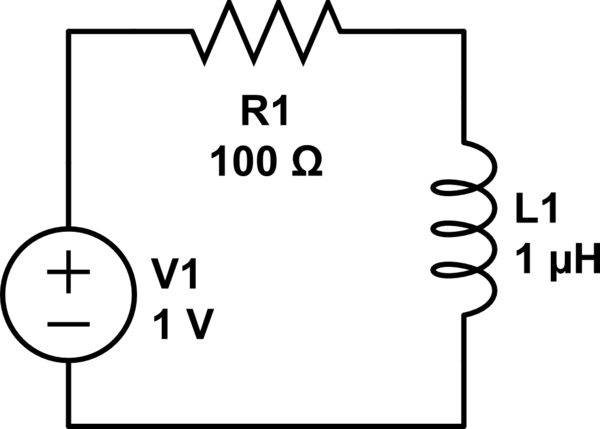
Consider a circuit consisting of a voltage source, a resistor, and an inductor arranged in a closed loop. When the voltage source is activated, the circuit reaches a steady state, during which the inductor stores energy calculated by the...
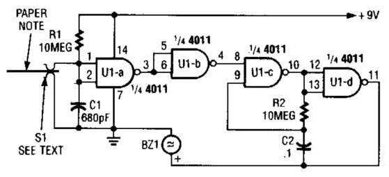
This device prevents paper notes and memos from being overlooked. A paper note placed between two fingers made of a conducting material (metal or conductive plastic) breaks the circuit, allowing pair 1 of Ul-a to go high. The goal...
This circuit generates a two-tone effect similar to the cuckoo song. It can be utilized for doorbells or other applications due to its integrated audio amplifier and loudspeaker. As a sound effect generator, it can connect to external amplifiers,...
The objective of this project is to control the speed of a DC motor. The primary benefit of utilizing a DC motor is the ability to modify the Speed-Torque relationship to nearly any desired form. To facilitate speed control,...
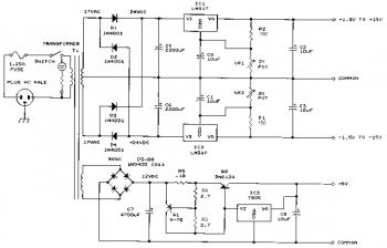
This bench power supply features three solid-state DC power supplies. The first supply provides an output of 1.5 to 15 volts at 1 ampere. The second supply offers a range of -1.5 to -15 volts at 1 ampere. The...