
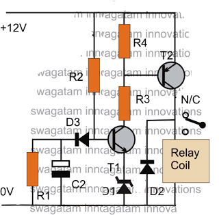
Monostable Multivibrator I Circuit

The described circuit features a transistor Q2, which acts as a switch or amplifier, depending on the configuration. When switch SW1 is pressed, it creates a path to ground for the base of Q2, causing the transistor to enter a conductive state. This activation allows current to flow from the collector to the emitter, thus controlling the load connected to the circuit.
The pulse rate of the circuit is determined by the time constant formed by resistor R3 and capacitor C1. The formula provided indicates that the pulse rate is approximately 0.7 times the product of these two components, which suggests that the circuit is likely configured as an astable multivibrator or a similar timing circuit. The values of R3 and C1 will dictate the frequency of the pulses generated.
In practical applications, the choice of R3 and C1 will affect the duration of the high and low states of the output signal. A larger resistance or capacitance will result in a slower pulse rate, while a smaller resistance or capacitance will produce a faster pulse rate. Additionally, the circuit may include other components such as diodes for protection, additional transistors for amplification, or operational amplifiers for signal conditioning, depending on the intended application.
Overall, this circuit can be utilized in various applications, including timers, pulse generators, or as part of a larger control system where timed events are necessary. Proper selection of components and careful layout design will ensure reliable operation and desired performance. This circuit is activated when SW1 is pushed to ground the base of transistor Q2. The pulse rate is approximately equal to 0.7(R3xCl). 🔗 External reference
Related Circuits
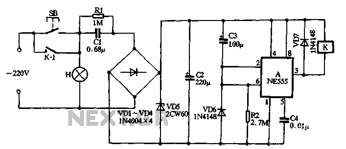
The NE555 push-button delay lamp circuit is illustrated in Figure 3-5. This circuit features several components, including a power supply and relay control system. Typically, the switch SB and normally open relay contacts K1 are in an open state,...
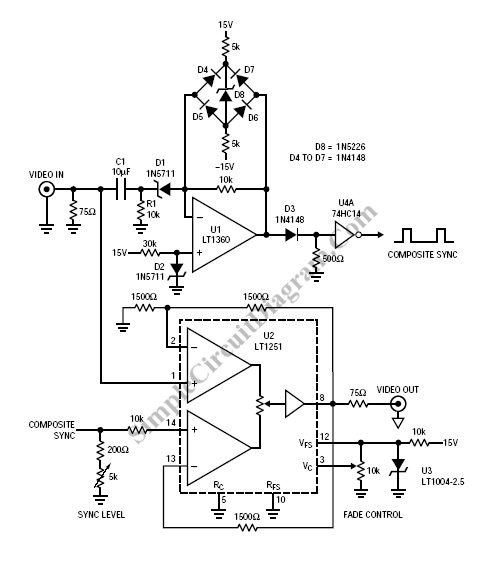
Fading a video signal cannot be achieved merely by attenuating the composite signal, as this may cause the synchronization signal to fall below an unacceptable level. To effectively fade a video signal while maintaining the integrity of the synchronization...
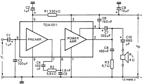
The following schematic illustrates the design of a 4 Watt Amplifier Circuit Diagram intended for portable radio applications, utilizing the TDA1011 integrated circuit from Philips Semiconductor. The 4 Watt Amplifier Circuit is designed to provide audio amplification in portable radio...

This project is suitable for individuals who enjoy experimenting with electronics. It presents a low risk of damaging the unit. This project involves creating a simple electronic circuit that allows users to engage in hands-on experimentation without significant risk. The...
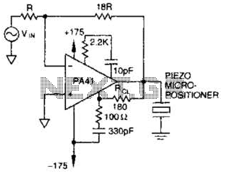
The PA41 from Apex Microtechnology is utilized to drive a piezoelectric micropositioner. The drive voltage is less than 20 V peak-to-peak at the input. The PA41 is a high-performance power amplifier designed specifically for driving piezoelectric devices, which require precise...
The post discusses a simple delay ON circuit that enables a connected load at the output to be activated with a predetermined delay after the power switch is turned ON. This circuit can be utilized in various applications that...
Warning: include(partials/cookie-banner.php): Failed to open stream: Permission denied in /var/www/html/nextgr/view-circuit.php on line 713
Warning: include(): Failed opening 'partials/cookie-banner.php' for inclusion (include_path='.:/usr/share/php') in /var/www/html/nextgr/view-circuit.php on line 713