
Mosfet circuit schematics
The described circuit examples highlight the differences in operational characteristics between bipolar junction transistors (BJTs) and metal-oxide-semiconductor field-effect transistors (MOSFETs). The first circuit, which incorporates a PNP and an NPN transistor, demonstrates the use of BJTs in switching applications. In this configuration, the PNP transistor is typically used to switch the positive side of the load, while the NPN transistor switches the ground side. The current consumption of 4.5 mA indicates that the BJT configuration requires a higher base current to maintain saturation compared to the MOSFET configuration.
In contrast, the second circuit utilizing two MOSFETs showcases the advantages of field-effect transistors in terms of efficiency. The significantly lower current draw of 0.1 mA is a result of the high input impedance of MOSFETs, which allows for minimal gate current. This characteristic makes MOSFETs ideal for applications where power consumption is critical, such as in battery-operated devices.
The schematic for the BJT circuit would include the PNP transistor connected to the positive voltage supply, with the load connected to the collector and the emitter grounded. The base of the PNP transistor would be driven by a control signal through a resistor. The NPN transistor would be connected similarly, with the load connected to the collector and the emitter grounded, and the base driven by the same or a complementary control signal.
For the MOSFET circuit, the schematic would depict two MOSFETs arranged in a similar manner, with the first MOSFET controlling the load connected to the positive supply and the second MOSFET providing a return path to ground. The gate of each MOSFET would be driven by a control signal, ensuring that they are turned on and off as needed with minimal gate current.
Overall, these examples illustrate the practical applications of BJTs and MOSFETs in electronic circuits, showcasing their respective advantages in current consumption and efficiency. Feedback on these designs would be beneficial for further refinement and optimization.Sid, I put together two working examples, one using a PNP and NPN transistor, and one using two MOSFETs. Both work fine, but as expected the MOSFET circuit consumes much less current (0.1 mA vs. 4.5 mA). Comments, suggestions, and bug reports gratefully received.. 🔗 External reference
Related Circuits
The electronic designs for the two animatronic mouths are presented below. The first design is for the articulated mouth, with additional servos for the eyebrows and eyes. The second design is for the LCD mouth, which closely resembles the...
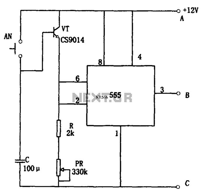
The circuit features a straightforward long timing mechanism. Activating switch AN initiates the timing process, while tone PR allows for timing adjustments. The timing range spans from 3 minutes to 220 minutes. With a capacitance value of 2200 µF,...
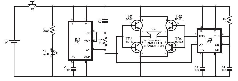
This ultrasonic sensor circuit consists of a set of ultrasonic receivers and transmitters that operate at the same frequency. When an object moves within the covered area, the circuit's balance is disturbed, triggering the alarm. The ultrasonic circuit is...
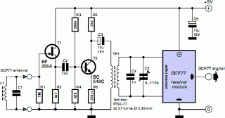
A popular project among microcontroller enthusiasts is to construct a radio-controlled clock. Compact receiver boards are available, equipped with a pre-tuned ferrite antenna, which can receive and demodulate the DCF77 time signal broadcast from Mainflingen, Germany. The DCF77 signal...
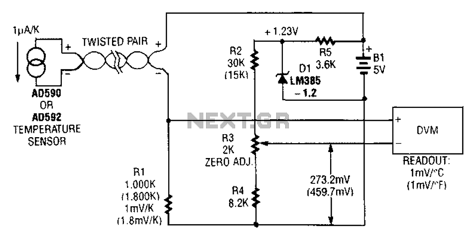
An AD590 or AD592 can be utilized in a transmission line for temperature data transmission. The circuit generates a value of 1 mV per degree Fahrenheit. The AD590 and AD592 are precision temperature sensors that output a voltage proportional to...
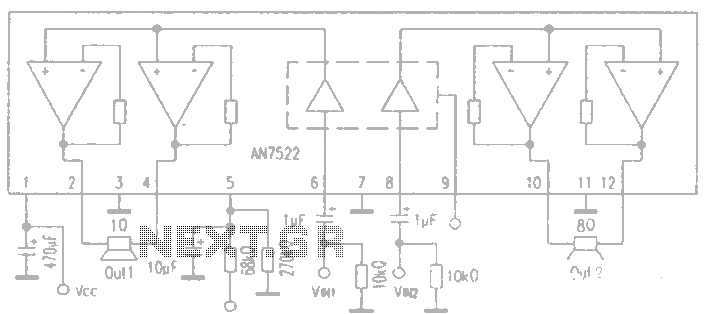
AN7522 is a Panasonic stereo audio amplifier IC that delivers an output power of 3W at 8 ohms. It features a standby function, low static power consumption, and reduced noise levels, requiring fewer external components for stable operation. This...