
MOSFET Headphones
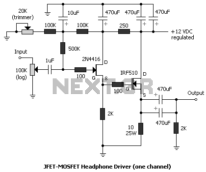
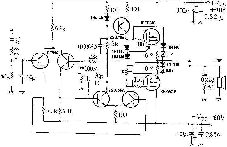
The described headphone buffer circuit is a sophisticated implementation of a zero feedback, class A amplifier configuration, utilizing MOSFET technology to drive low impedance headphones effectively. The design is predicated on the principles established by Greg Szekeres, emphasizing the importance of a robust power supply and appropriate coupling strategies to maintain audio fidelity.
The circuit operates within a voltage range of 12-15V, making it specifically tailored for low impedance headphones, such as the 32-ohm Grado SR60s. The choke-regulated power supply is integral to the performance, minimizing high-frequency noise and providing a cleaner signal than traditional voltage regulator ICs. This is achieved by employing a choke input design, which ensures that ripple voltage remains low, measured at approximately 3mV rms, with negligible high-frequency noise.
The input stage utilizes a JFET follower, which presents a low output impedance, allowing for a flat frequency response that is crucial for accurate audio reproduction. The design incorporates an output coupling capacitor configuration that significantly impacts the amplifier's frequency response. The use of two unbypassed low impedance 470uF electrolytic capacitors in parallel allows for a minimal roll-off at high frequencies, maintaining a frequency response of 20-20kHz ±0.2 dB.
Biasing is carefully managed, with trim pots allowing for adjustment to ensure balanced voltage levels across the MOSFETs. The bias voltage at the source of the JFET is approximately 5.5V, while the gate voltage of the MOSFET is around 7.5V, providing sufficient headroom for the circuit to operate without distortion, as long as input signals remain below 1V rms.
The design also incorporates critical components such as gate resistors, which smooth the output and can be adjusted to modify the amplifier's tonal characteristics. The interaction between the gate resistor and the MOSFET's input capacitance forms a low-pass filter, allowing for tailored adjustments to the treble response. Coupling capacitors play a vital role in defining the amplifier's sound quality, with selections based on both type and value being essential for achieving the desired audio characteristics.
In conclusion, this headphone buffer circuit exemplifies the importance of component selection and circuit design in audio applications, ensuring that low impedance headphones receive a high-fidelity signal with minimal distortion and an extended frequency response. The careful consideration of the power supply, coupling methods, and biasing strategies collectively contribute to the overall performance and sound quality of the amplifier.This headphone buffer is based on Greg Szekeres' MOSFET Headphone Driver. It is a robust and reliable zero feedback, class A circuit. [Editor: And like the Szekeres MOSFET amp, this amp has unity voltage gain. Therefore, the audio source must supply adequate voltage to drive headphones.] The power supply is choke regulated. The circuit is configured for low impedance headphones like my 32-ohm Grado SR60s. Greg's circuit was designed to be driven from the output of a preamplifier, as high frequency rolloff will result when a volume control feeds directly into the IRF510 MOSFET, due to the MOSFET's high input capacitance.
If a signal from the volume control feeds directly into an IRF510 MOSFET, there will be a high frequency rolloff due to the MOSFET's high input capacitance. Contrary to popular belief, the output coupling capacitor is not the source of the limited high frequency response.
Two unbypassed low impedance 470uF electrolytics were used in parallel, and the response was less than a quarter of a dB down at 50 kHz! The output impedance of the JFET follower is only a few hundred ohms, so it drives the MOSFET with a flat frequency response.
Since it has a very low input capacitance, a 100 kOhm volume control can be used without penalty. A flat frequency response translates into less coloured, more realistic sound (though not necessarily the most likeable). The frequency reponse of this amplifier, measured with a real load (Grado SR60s), is 20-20kHz ±0.2 dB.
The amp's output impedance is a constant 3 ohms. This amplifier project took more time than I expected. I am more familier with tube circuits, and the learning curve for solid state circuitry was steep. What I had not properly understood was how critical power supply design is, for high current circuits like this. Voicing this amp is all about the power supply. The amp had been at the "good but not perfect" stage for several months. I made changes, improvements even, but I did not nail it until I concentrated on the power delivery channel, (a.k.a.
the region between the power supply and the signal circuit). The power supply has a choke input and sounds better than a regulated supply. A choke input is used in the power supply to prove that this arrangement can and does sound better than voltage regulator ICs. Observing the supply voltage on an oscilloscope, the ripple is a 120Hz sinewave about 3mV rms: high frequency noise components so pernicious in regulated supplies are absent.
The operating voltage for this circuit is 12-15V, which means that it is only suitable for driving low impedance headphones (60 ohms of less) like those made by Grado. High impedance headphones need more voltage headroom. The trim pots on the bias supply can be adjusted to get the voltage at the source of the mosfet equal for both channels, but the JFETs may require matching to get the voltages roughly equal first.
The bias voltage is about 5.5V, the source of the JFET, directly coupled to the gate of the MOSFET is about 7.5V, and the source of the MOSFET is about 3.5V. This ensures sufficient headroom, as long as the signal isn't above 1V rms. The source resistor on the MOSFET can be any value between 10 and 30 ohms. Just remember as the value goes down, current demand and heatsinking requirements go up. The two 100 ohm gate resistors are important. The sound is smoother with them in, so leave them in. The frequency response of the amp can be adjusted to taste. The MOSFET's gate resistor acts with the MOSFETs input capacitance to create a low pass filter. Increasing the value of the gate resistance will cool off a bright or too prominent treble. The bass response can be rolled back by removing one of the output coupling capacitors, or decreasing the capacitance value.
Adding more capacitance does not increase the bass, but reducing the treble as described above will subjectively produce more bass. There are many other changes which are audible but not measurable. The quality of the coupling capacitors for example. The amp's sound is affected by the type as well as the value of the coupling capacitors. I use Sprague "orange drop" 225P 1.0uF / 100V on the input. Although they are metallized polyester, they sound warm and natural. 0.47 uF or 1.0 uF polypropylene (such as the Solen caps) would be interesting alternatives. Exotic audio-specific upgrades may be worthwhile. I recommend trying low inductance electrolytic capacitors, such as the inexpensive Panasonic FC series (available from Digikey) for the output.
The output coupling capacitors must be electrolytic. If big, standard types are used, the sound will be muddy and distorted. Bypassing generic electrolytic caps does not work: the sound is still muddy and distorted, with added high frequency noise. I've tried various configurations and settled on using parallel, unbypassed, low-inductance electrolytics.
Every major manufacturer makes them, as they are used in switching power supplies. Mine were United Chemi-Con SXC. 1000uF was better than 470uF, but 2x470uF was best. Adding more was not of further benefit. As the low inductance caps are quite comfortable up to 100 kHz, there is no need to bypass them, and indeed they sound better that way. The ripple is fairly high, however, and unless the bias voltage to the gate of the JFET is carefully filtered, there will be audible hum.
A 500K resistor separates the gate from the voltage divider, and a 10 uF cap bypasses the bottom half of the divider, shunting the ripple on the bias voltage to ground. Ripple at the output (0.3 mV rms estimated) is barely visible on the ‘scope, and not audible. 🔗 External reference
Related Circuits
This solid-state switch detects and interrupts an overcurrent condition within 2 microseconds. It allows the circuit to float. IC1 operates at 150 kHz, and the full-wave doubler D1/D2 provides 15 V to the gate of Q1. An overcurrent sensed...
A new enthusiast in electronics has recently taken up the hobby, having built a few guitar pedals and small amplifiers. The current project involves a new electronic device. The project may involve designing a circuit that incorporates various components typical...

If the total circuit resistance can be significantly reduced to less than 0.1 Ohm and a load of 0.4 Ohm or less is connected, over 1 kilowatt of free electrical energy can be obtained. There are two discrete voltage...
A Common Cathode LED strip is being utilized instead of a Common Anode variant, leading to the development of a modified circuit. The experience with FETs was limited, resulting in challenges as a minimum voltage equal to Vcc is...
Using measured threshold voltage and Ids-Vds curves, the performance of first-order MOSFET theory can be evaluated in real devices, allowing for an understanding of the limitations of first-order theoretical MOSFET equations. The MOSFETs employed in this experiment are from...
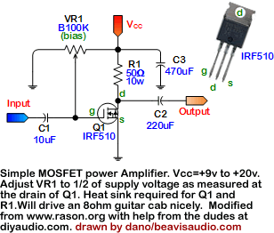
Currently, a basic MOSFET amplifier or power amplifier is designed to deliver an output power of ±100 Watts RMS with an 8 Ohm load, or ±160 Watts RMS with a 4 Ohm load. The simplicity of this circuit results...
Warning: include(partials/cookie-banner.php): Failed to open stream: Permission denied in /var/www/html/nextgr/view-circuit.php on line 713
Warning: include(): Failed opening 'partials/cookie-banner.php' for inclusion (include_path='.:/usr/share/php') in /var/www/html/nextgr/view-circuit.php on line 713