
Power Mosfet Switch

The described solid-state switch is engineered to provide rapid overcurrent protection in electronic circuits. The operation begins with the sensing mechanism that monitors the current flowing through resistor R1. When the current exceeds a predetermined threshold, the voltage across R1 rises, triggering transistor Q3. This transistor acts as a control switch, which, upon activation, cuts off the gate bias to Q1, effectively disconnecting the load from the power source.
The use of a full-wave bridge rectifier comprising diodes D1 and D2 ensures that the circuit can efficiently convert AC input into a stable DC output. The output voltage of 15 V is crucial for driving the gate of Q1, which is typically a MOSFET or an IGBT, allowing for rapid switching capabilities. The frequency of operation, set at 150 kHz, indicates that the circuit can handle high-speed applications, making it suitable for various industrial and consumer electronics.
Capacitor C1 and resistor R3 are integrated into the design to provide additional robustness against voltage surges. C1 functions as a decoupling capacitor, smoothing out voltage spikes that could potentially harm sensitive components. R3 serves to limit the inrush current during transient conditions, ensuring that the circuit remains stable under fluctuating load conditions.
Overall, this solid-state switch design exemplifies modern approaches to circuit protection, utilizing rapid response times and efficient power management techniques to enhance the reliability and durability of electronic systems. This solid-state switch senses and interrupts an overcurrent condition within 2 /is. II allows the circuit to float. IC 1 runs at 150 kHz and full-wave doubler D1/D2 provides 15 V to the gate of Ql. An overcurrent sensed across Rl triggers Q3, removes gate bias from Ql, and opens the circuit formed by the full-wave bridge and Ql. CI and R3 allow the circuit to handle surges.
Related Circuits

The AA-7 active antenna consists of two active components: Q1 (an MFE201 N-channel dual-gate FET) and Q2 (a 2SC2570 VHF silicon transistor), which form the foundation for two independent, switchable RF preamplifiers. The AA-7 active antenna is designed to enhance...
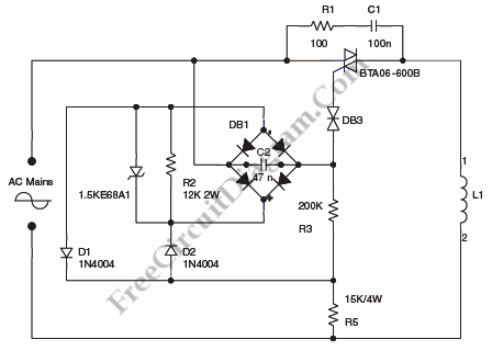
A step-down circuit is utilized to approximately halve the RMS voltage between the line input and the inductive load (L1), as illustrated in the circuit diagram below. A turn-on delay of about 7 ms is achieved through the combination...

UPDATED 2014 This project presents the original high-power mobile phone jammer circuit, with all updates posted here. Caution is advised regarding the use of this device, as it is illegal. The purpose of sharing this circuit is solely for...
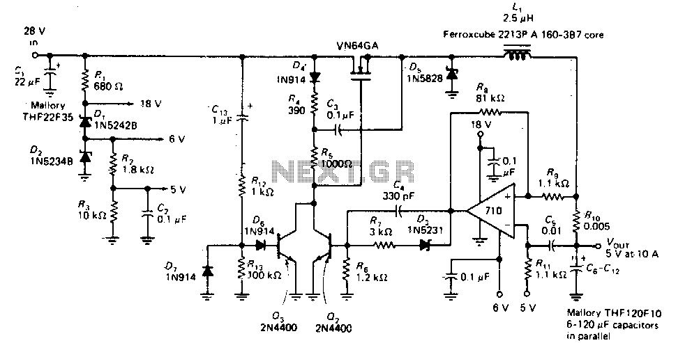
This circuit provides a regulated DC output with less than 100 mV of ripple for microprocessor applications. The required operating voltages are derived from a bleeder resistor network connected across the unregulated 28 V supply. The output of the...
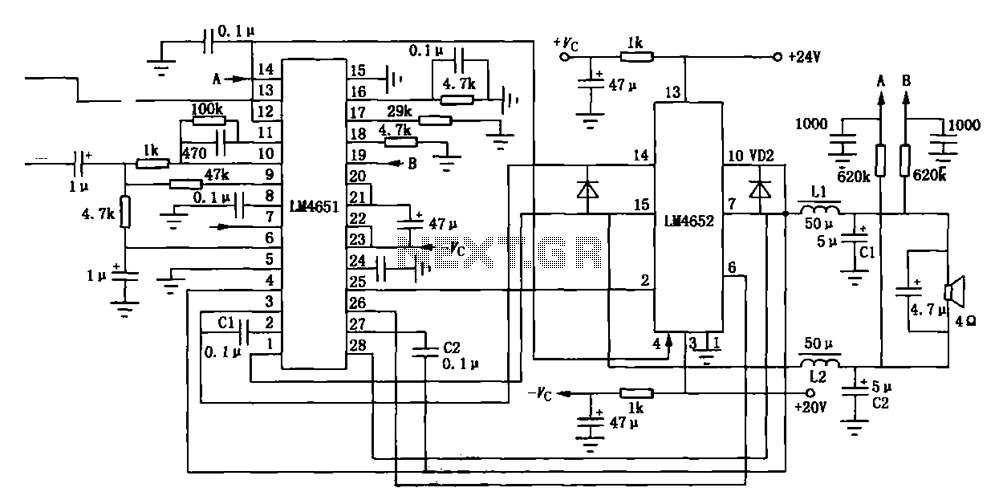
Figure (a) illustrates a 170W output amplifier circuit designed for a 4-ohm load. The LM4651 is a class D amplifier presented in a 28-pin DIP package, with its internal equivalent circuit depicted in Figure (c). The 170W output amplifier circuit...
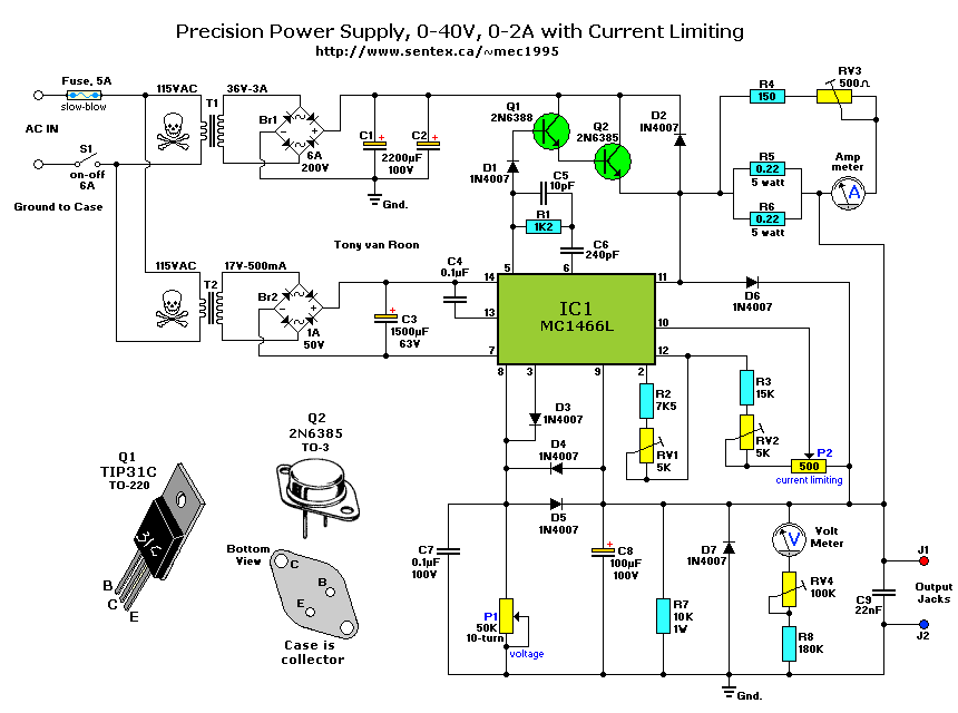
This precision power supply is a valuable addition to any workbench, serving as either a primary or supplementary power supply. It offers a voltage range of 0 to 40V and a current capacity of 2A, with adjustable current limiting...