
Mosfet Wideband Amplifier

In high-impedance applications, the described amplifier configuration utilizes a Field Effect Transistor (FET), specifically the 40673 model, which exhibits a transconductance (gm) of approximately 12 mS (12 x 10^-3 S). The voltage gain of the amplifier is determined by the relationship between the transconductance and the load impedance (ZL). The formula -gm/ZL indicates that as the load impedance increases, the voltage gain becomes more negative, reflecting an inverting amplifier configuration.
The amplifier's performance can be fine-tuned through the G2 voltage, which serves as a control voltage for the gain. By adjusting this parameter, the user can manipulate the transconductance of the FET, thereby altering the output voltage level in response to a given input signal. This feature is particularly useful in applications requiring precise gain control, such as in instrumentation or audio amplification.
For optimal operation, it is essential to ensure that the load impedance is well-defined and that the FET operates within its specified parameters. Careful consideration of the power supply voltage and biasing conditions will also contribute to the overall performance of the amplifier circuit. The design should incorporate sufficient decoupling capacitors to minimize noise and ensure stability, particularly in high-frequency applications. For high-impedance (7 500 ) applications, this amplifier will provide a voltage gain of approximately -gm/ where ZL is the load impedance in ohms and gm is ~ 12 10~3 for the 40673 FET. The G2 voltage can be used to control the gain. 🔗 External reference
Related Circuits
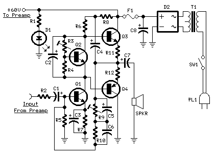
This design utilizes a well-established circuit topology for the power amplifier, employing a single-rail supply of approximately 60V and capacitor coupling for the speakers. The advantages of this configuration for a guitar amplifier include a straightforward circuit design, even...
This diagram originates from the Progressive Communications Receiver featured in most recent ARRL Handbooks. The amplifier is utilized wherever an intermediate frequency (IF) amplifier is necessary. W6BKY has published an article on Hamradio-online that details the construction of this...
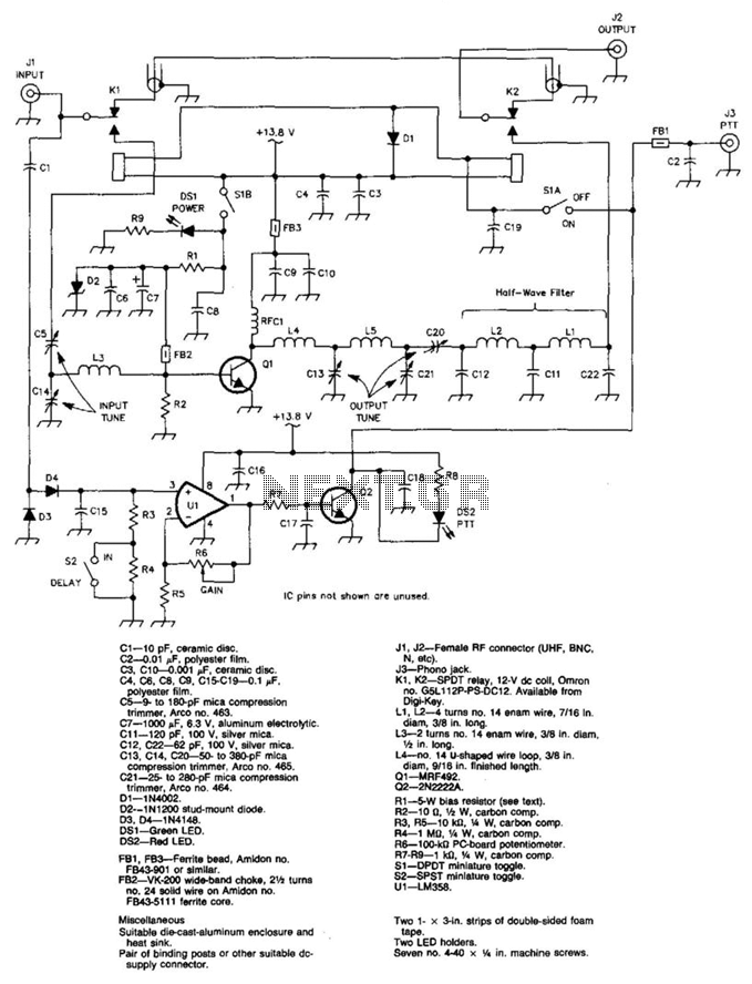
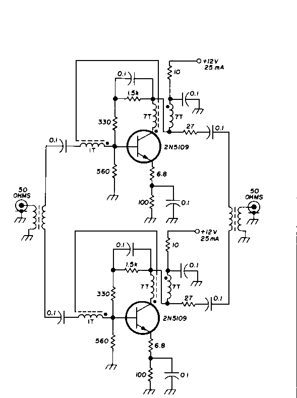
A 100 W output at 50 MHz is available from this circuit. U1 and Q2 form a T-R relay driver, switching the amplifier on when RF input at J1 is sensed. During receive periods, J1 and J2 are directly...
This simple audio power amplifier was originally designed for a circuit board workshop conducted by the OSU IEEE Student Group. At the workshop, 20 participants each constructed this amplifier by etching and drilling the single-sided circuit board, soldering all...
The video amplifier circuit utilizes the LM359 integrated circuit, which is a dual, high-speed, programmable current mode (Norton) amplifier. This circuit is suitable for general-purpose video amplification applications. The LM359 is designed to operate as a high-speed amplifier, making it...
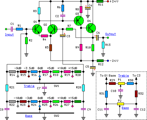
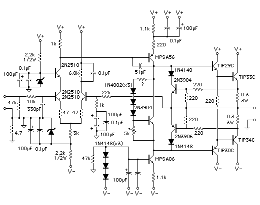
High-quality, discrete component design for input and tone control modules to complement the 60-watt MOSFET audio amplifier with a high-quality preamplifier design. The circuit design focuses on creating a high-fidelity audio preamplifier that enhances the performance of a 60-watt MOSFET...