
Motorola SN54 Demultiplexer Logic Diagram and Datasheet
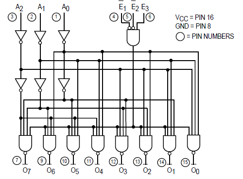
The Motorola SN54/74LS138 is a high-speed CMOS logic device that operates as a 1-of-8 line decoder/demultiplexer. This component features three binary select inputs (A0, A1, A2) that can decode a 3-bit binary number into one of eight active low outputs (Y0 to Y7). The device also includes three enable inputs (G1, G2A, G2B) which must be appropriately activated to allow the decoder to function. When the enable inputs are not activated, all outputs remain inactive regardless of the select input states.
The operational speed of the SN54/74LS138 makes it suitable for applications requiring rapid address decoding, such as in memory chip selection for microprocessors. The architecture of the device allows for cascading multiple SN54/74LS138 chips to expand the decoding capability. By connecting four of these devices along with a single inverter, one can achieve a 1-of-32 decoding scheme. This is accomplished by using five input lines to select one of the thirty-two outputs, effectively increasing the number of selectable outputs while maintaining the high-speed performance characteristic of the SN54/74LS138.
In practical applications, the multiple enable function enhances versatility in circuit design, allowing for complex configurations without significant additional components. The logic diagram of the SN54/74LS138 can be utilized to understand the internal workings of the device, including the AND gates and inverters used to produce the desired output based on the binary input. This makes the SN54/74LS138 a crucial component in digital systems requiring efficient address decoding and demultiplexing capabilities.Motorola SN54/74LS138 known to be 1-of-8 decoder or demultiplexer which is designed for high speed bar memory chip select address decoding. Below diagram illustrates logic diagram of this SN54/74LS138 demultiplexer. According to the SN54 datasheet, multiple enable function allows easy parallel expansion of the device to a 1-of-32 (5 lines to 32 li
nes) decoder with just four LS138s and one inverter. Diagram 🔗 External reference
Related Circuits

The LMP91200 is a configurable sensor analog front-end (AFE) designed for managing low-power analytical sensing applications, specifically for 2-electrode sensors. This device offers all the necessary functionality to detect changes based on a delta voltage from the sensor. It...
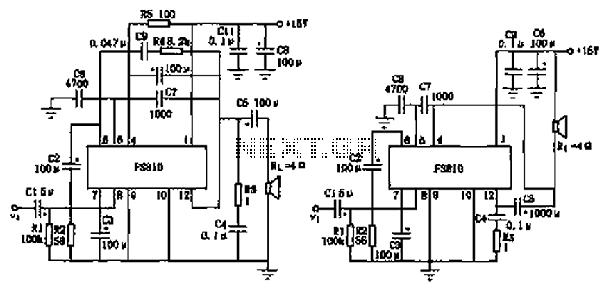
The FS810 circuit serves as a practical implementation of an integrated power amplifier. The FS810 is designed for high-performance use in high-end tape recorders and audio equipment. In the schematic, the speaker is connected to the output capacitor C5...
The LM324N is part of the LM324 family, which includes four independent, high-gain, internally frequency-compensated operational amplifiers. These amplifiers are designed to operate from a single power supply over a wide range of voltages. Operation from split power supplies...
The Boss SD-1 Super OverDrive is a pedal characterized by a straightforward design, incorporating a dual operational amplifier (uPC4558C) and six transistors, along with an asymmetric overdrive circuitry that emulates the classic, natural growl of a tube amplifier. It...
Instructions for supervising landscaping projects recommended by satellite relay protection and automatic safety devices. This includes information on the general table for three remote programs related to petrochemical engineering construction, electrical transmission, and the intelligent implementation of community weak...
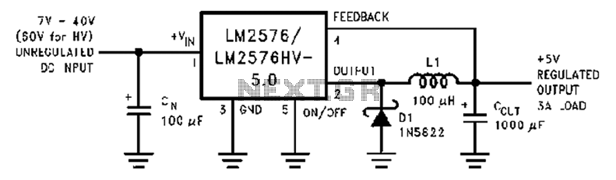
A wide range of 7 to 40V DC-DC step-down circuit that converts input voltage to 5V. This circuit operates as a buck converter, designed to efficiently reduce a higher DC voltage (ranging from 7V to 40V) to a stable output...