
Motorola TPN1154 and TPN1136 Desktop Power Supplies
The circuit design involves several key components, including the LM7812 voltage regulator, transistors (Q1, Q2, Q3, Q4, Q5), resistors (R1, R12, R13), and a variable resistor (VR1). The LM7812 serves as the primary voltage regulation component, providing improved line regulation compared to the original design. The transistors function as amplifiers and switches, working together to maintain the output voltage within specified limits. The resistors form part of the feedback loop, helping to stabilize the output voltage against fluctuations in load and input voltage. The variable resistor allows for fine-tuning of the output voltage, accommodating variations in component tolerances and ensuring that the output remains within the desired range.
The schematic layout should reflect the connections between these components clearly, illustrating how the unregulated voltage from the AC input is transformed into a stable regulated output. The importance of proper grounding and component placement cannot be overstated, as these factors significantly influence the performance of the circuit. The design should also include provisions for heat dissipation, particularly for the LM7812 and power transistors, to prevent thermal overload and ensure reliable operation. Overall, the redesigned power supply circuit aims to enhance performance, stability, and adjustability, providing a more robust solution for the intended application.The regulated output voltage varied as the unregulated DC voltage changed, and that changed as the load current or the incoming AC line voltage was varied. There was no easy fix to the existing circuit that would solve this problem. Eric WB6FLY had already run some load tests on these supplies and mine acted just like his did. The problem is that the unit is designed poorly. The unregulated DC voltage is used to provide power for the regulator circuit and that voltage decreases as the load current increases, so the regulation suffers. Varying the incoming AC line voltage also changes the unregulated DC voltage, so it too has just as much effect on the regulated output voltage.
The graph below shows how bad things are. I did some investigation and noticed that the line regulation spec for the common LM7812 three-terminal regulator is in the order of tens of millivolts, far better than what the Motorola power supply was ever capable of producing. The downside is that these three-terminal regulators are only capable of about 1 amp of current, far less than the Motorola power supply was designed to do.
Studying the data sheet, I think I figured out a way to use an LM7812 regulator in place of most of the original regulator circuitry. I tried to implement this as a drop-in replacement, where the original circuit board is removed and a new one with a few simple parts is installed.
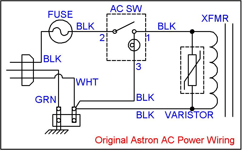
The original supply was non-adjustable; I decided to make mine adjustable, at least within about +/- 15% of the nominal 14VDC output. I did all of this for a parts cost of under $7US. Here`s the original schematic of the 14-amp power supply, taken from the Maxar-80 manual. The 8-amp supply has only one series regulator transistor (Q4) that feeds the output directly; it does not have R12 or R13, or Q5 mounted to the heat sink.
The regulator circuit board components are shown in the schematic to the left of the terminal strip, in the area surrounded by dotted lines. Here`s a photo showing the terminal strip and the original regulator circuit board. The terminals are numbered sequentially from 1 to 8, starting at the front of the supply (left side of photo).
Lugs 2 and 7 are used to mount the terminal strip, which grounds them. Lug 4 is unused. The terminal strip lugs have the following use or function. Note that the Wire Color is the color of the wire that goes from the terminal strip to the regulator circuit board. The regulated output voltage enters the regulator circuit board at pin 8. If this voltage is too low, Q2 will draw less current through R1 and its collector voltage will rise.
This causes Q1 to draw more current, pulling the base of Q3 lower, causing Q3 to draw more current, which pulls the bases of Q4 and Q5 higher, causing them to pass more current to the load, which causes the voltage at pin 8 to rise. This returns the circuit to equillibrium. If the regulated output voltage rises, Q2 turns on more, Q1 draws less current, Q3 draws less current, Q4 and Q5 pass less current, and the output voltage decreases, restoring equillibrium.
Unfortunately the unregulated input voltage that comes into the board at pin 6, also has an effect on the regulated voltage. This can drop because the incoming AC voltage goes lower, or when the load current increases. Thus the current feeding VR1 varies as a function of both the load current and the line voltage; hence the poor regulation.
I just unsoldered six wires at the circuit board so I could attach them to the new regulator circuitry. On my unit, Q3 was a TO-220-style transistor but its White-Brown collector lead went to a circuit board pad where the other White-Brown wire coming from the terminal strip was attached, rather than going directly to lug 3 of the terminal strip as implied in the schematic, so I attached the White-Brown wire to lug 3.
Leave the other wires going to Q3. See the clos 🔗 External reference
Related Circuits
The adaptive adjustable power supply is illustrated in the accompanying figure. The power supply utilizes an LM317 regulator device, and an adaptive switching circuit that automatically adjusts the input voltage based on the output voltage level. This mechanism reduces...
If you plan to use this circuit with a 110V 60Hz supply instead of a 230V 50Hz supply, or if you intend to modify this circuit, please refer to the section titled "Common Questions about this Circuit" found below...
A compilation of dial phone numbers, including 15 commonly used libraries and the dialed number, is stored in standard CMOS RAM. A single-button keypad facilitates the input of a phone number, which can be dialed directly or stored in...
300W Subwoofer Power Amplifier. High power amplifiers are not common as projects, as they are inherently challenging to build and often expensive. A minor error during assembly can lead to significant issues. The 300W subwoofer power amplifier is designed to...
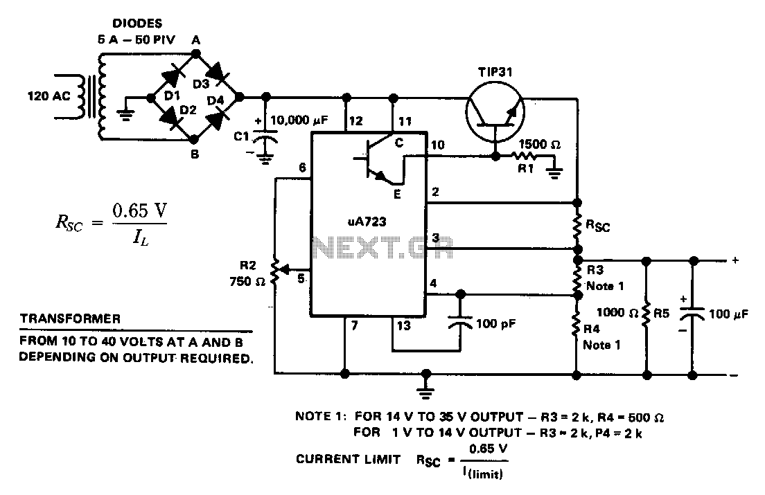
The supply 6-66 can be utilized for output voltages ranging from 1 to 35 V. The line transformer must be selected to provide approximately 1.4 times the desired output voltage from the positive side of filter capacitor C1 to...
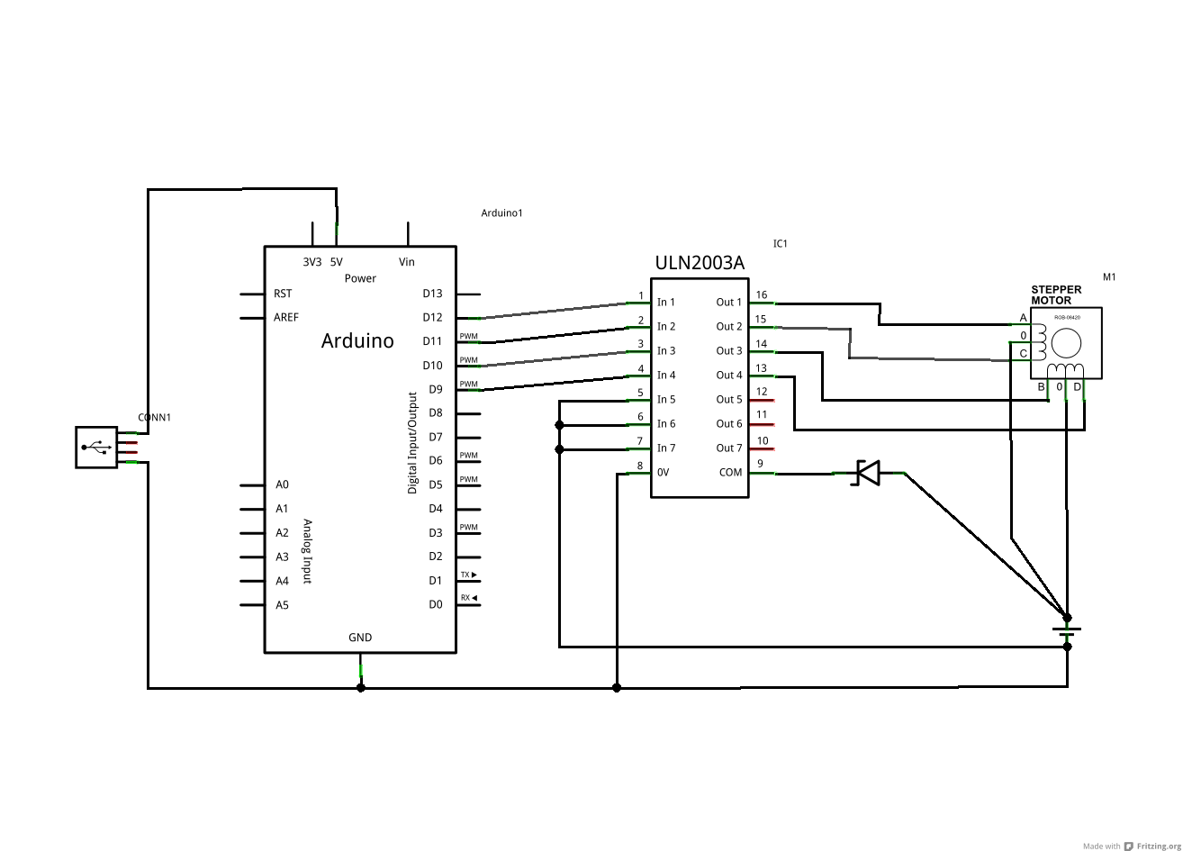
The ULN2003A and Zener diode are components from the driver board within the same device. The motor in question has five wires, while the schematic depicts a six-wire motor. It is assumed that the difference lies in the fact...