
Large Lcd Display Buffering Driver Circuit

The circuit design incorporates a series of operational amplifiers configured as buffer amplifiers to effectively drive large LCD displays. Each buffer amplifier is strategically placed to manage the common lines, which helps to mitigate the effects of high driving capacitance. The ability to program each amplifier independently allows for fine-tuning of the quiescent current, which is essential for optimizing performance based on the specific requirements of the display.
The bias network plays a critical role by establishing a consistent voltage that sets the quiescent current to 100 µA across all three amplifiers. This uniformity helps maintain stable operation and ensures that the amplifiers function within their optimal ranges. The operational amplifiers are designed to operate within a voltage range of 5 V to ground, accommodating the varying common signals that range from 5 V down to approximately 1 V.
To protect the integrity of the signals processed by the amplifiers, an attenuation mechanism is employed, reducing the signal amplitude by half. This strategy ensures that the common-mode voltage remains within the acceptable limits of the operational amplifiers, thereby preventing distortion or signal clipping. The buffer amplifiers are configured to provide a gain of two, which allows for adequate signal amplification while preserving the fidelity of the input signals.
The circuit is capable of driving eight 1-inch LCD displays simultaneously, making it suitable for applications requiring multiple display outputs. It is designed to perform reliably under ambient temperature variations of 15 °C or less. In scenarios where the temperature approaches the upper limits, adjustments to resistor R1 are necessary to eliminate any visibility of off segments, ensuring that the display remains clear and legible under varying environmental conditions. This attention to detail in the circuit design enhances the overall performance and reliability of the LCD display system. Large LCD devices of 1 or more exhibit a large driving capacitance to the driver circuits. To solve this problem, the drive circuit shown (see the figure) introduces a buffer amplifier for each of the three common lines. Each amplifier can be programmed independently for a quiescent current of 10, 100, or 1000 jllA. In this application, the bias network applies a voltage that sets the three quiescent currents to 100 uA.
The display driver and triple op amp operate between 5 V and ground, and the COM signals range from 5 V to ~ 1 V. To ensure that these signals remain within the amplifiers` common-mode range, the signals are attenuated by one-half and the buffers operate at a gain of two.
The circuit drives eight 1-inch displays, and is suitable for ambient temperature variations of 15uF or less. At the highest expected temperature, R1 should be adjusted so that no off segments are visible.
Related Circuits
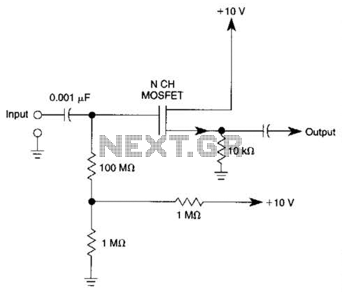
Biasing methods for an N-channel MOSFET to form a unity-gain noninverting amplifier or source-follower. The N-channel MOSFET can be utilized in various configurations, with one common application being the unity-gain noninverting amplifier, also known as a source-follower. In this configuration,...
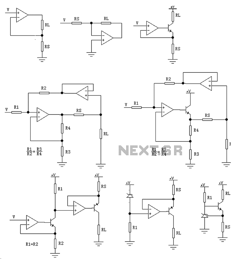
The circuit is designed to provide several constant current outputs to the load resistor RL. The first RL is floating and is rarely utilized. The second RL serves as a virtual ground and is not commonly used either. The...
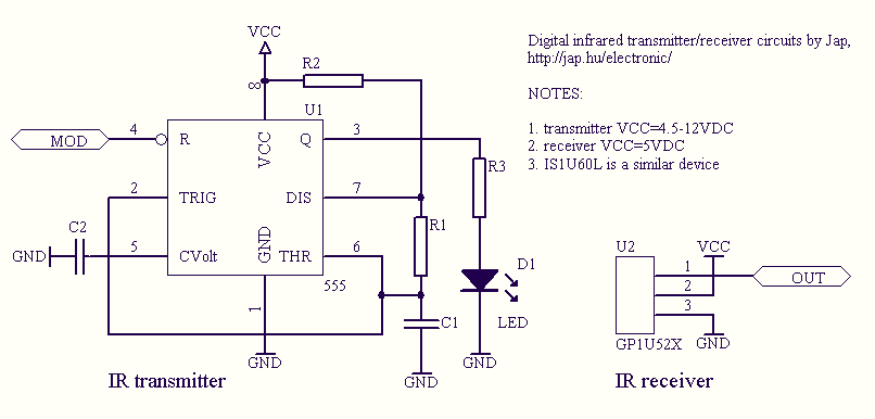
Infrared remote controls are using a 32-56 kHz modulated square wave for communication. These circuits are used to transmit a 1-4 kHz digital signal (OOK modulation) through infra light (this is the maximum attainable speed, 1000-4000 bits per sec)....
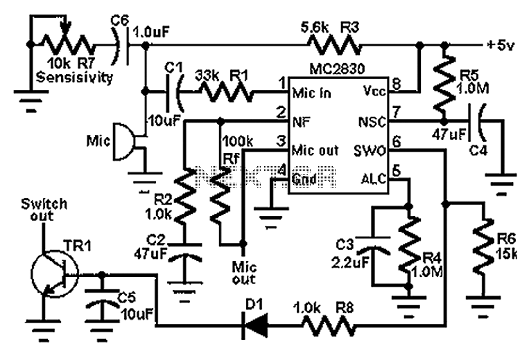
The circuit schematic utilizes the MC2830 voice circuit. Traditional voice circuits are unable to differentiate between speech and noise in the input signal. In noisy environments, such as those caused by switches, this limitation is significant. To address this...
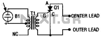
The photo strobe slave trigger circuit utilizes a solar cell and a silicon-controlled rectifier (SCR) to activate any strobe light when triggered by a master strobe. The small solar cell generates a minimal voltage when illuminated. The photo strobe slave...
This AC drill speed controller circuit schematic allows for the control of the drilling speed of a borer or drilling machine. This project is based on the principle that... The AC drill speed controller circuit is designed to modulate the...