
multi purpose flip flop timer
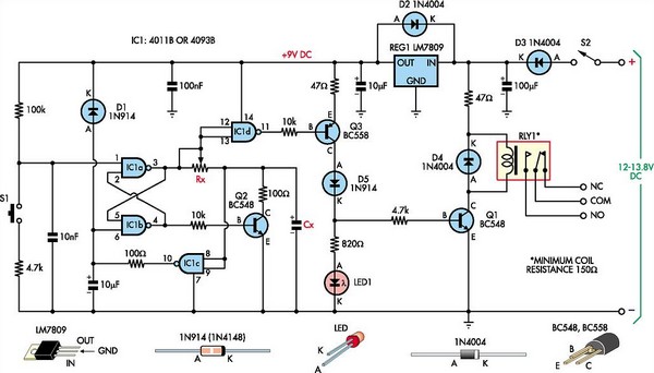
The circuit operates effectively by utilizing a combination of a CMOS NAND gate and a set/reset flip-flop configuration, allowing for precise timing control. The activation of the timing sequence through switch S1 initiates a charge cycle for capacitor Cx, which is critical in determining the timing duration. The use of a potentiometer for Rx provides flexibility in adjusting the timing delay, accommodating different application requirements.
The design ensures low power consumption in standby mode, making it suitable for battery-operated devices or applications where power efficiency is crucial. The protection mechanisms, including diodes D1 and D4, enhance the reliability of the circuit by preventing damage from voltage spikes and ensuring correct operation during power-up.
The choice of components, such as the CMOS 4011 and transistors, reflects a balance between cost and performance, making this timing circuit an economical solution for various timing applications. The straightforward formula for calculating the timing delay simplifies the design process for users, allowing for quick adjustments to meet specific timing needs. Overall, this circuit provides a robust solution for timing applications with minimal power consumption and user-friendly adjustability.This particular timing circuit can be used to time one-shot events from a few seconds to a few hours. And in standby mode (ie, with RLY1 and LED1 off), its power consumption is very low. The heart of this circuit is a low-cost CMOS 4011 quad NAND gate, with IC1a & IC1b configured as a standard Set/Reset flip-flop.
Briefly pressing switch S1 to sta rt the timing sequence pulls pin 1 of IC1a low and, as a result, pin 3 switches high. Two things happen while pin 3 is high: capacitor Cx begins charging via potentiometer Rx; and (2) pin 11 of IC1d will be low, which means that transistors Q3 and Q1 are both on. As a result, both LED 1 and relay RLY1 are also on. RLY1 and LED 1 remain on until Cx has been charged up to about 70% of Vcc (ie, the supply rail). At this point, pins 8 & 9 of IC1c are pulled high and so its pin 10 output goes low and resets the flip-flop by applying a low to pin 6 of IC1b.
This causes pin 3 of IC1a to go low and so LED1 and RLY1 switch off and the timing period ends. At the same time, pin 4 of the flip-flop goes high and this turns on transistor Q2 while ever the flip-flop is held reset. This ensures that Cx is discharged, so that the circuit is ready the next time S1 is pressed. Diode D1 and its associated 10 µF capacitor reset the flip-flop when power is first applied, so that LED1 and RLY1 remain off until S1 is pressed.
D4 is included to protect Q1 against the back-EMF that`s generated when the relay switches off. Choosing appropriate values for Cx & Rx for a given time delay is straightforward. The formula is T = 1. 24 x Rx x Cx, where T is the delay time in seconds. As an example, let`s assume that we require a time delay of 10s using a value of 100 µF for Cx. Now we just need to calculate the value of Rx as follows: In this case, an 82kO resistor would be the closest value. You can use either a fixed resistor for Rx or you can use a potentiometer (or trimpot) which can be adjusted to give the required time delay.
Note that the value of Rx should not be any more than a few megohms. Power for the circuit can be derived from any 12V DC source. This is then fed to 3-terminal regulator REG1 to derive a 9V rail to power the circuitry. The exception here is the relay circuit, which is powered from the 12V rail. Diode D3 protects the circuit against incorrect supply polarity. 🔗 External reference
Related Circuits
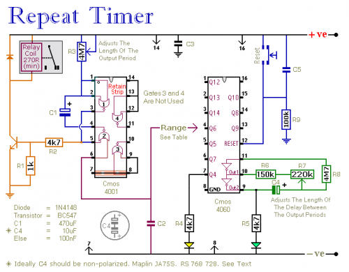
This circuit features an adjustable output timer capable of re-triggering at regular intervals. The output duration can range from a fraction of a second to half an hour or longer, with the ability to recur at intervals spanning from...
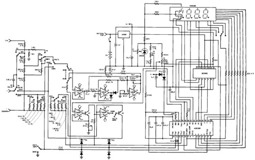
The following circuit illustrates the design of a simple digital multimeter circuit diagram. This circuit employs the ADD3501. Features include the combination of voltage measurements, among others. The circuit design for a simple digital multimeter utilizing the ADD3501 integrates several...
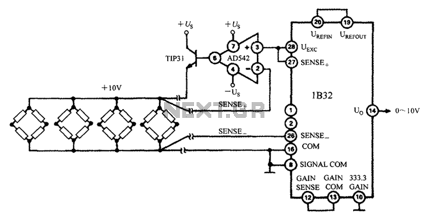
The 1B32 application circuit features multiple pressure sensors as illustrated in the figure. Excitation power is supplied through the AD542, which is followed by a TIP32 transistor that drives multiple bridge sensors. The AD542 operates as a Bi-FET in...
The circuit can be arranged in a circular format to represent the 12 hours of a clock face, with an additional 12 LEDs positioned in an outer circle to indicate 5-minute intervals within each hour. Four extra LEDs are...
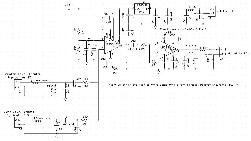
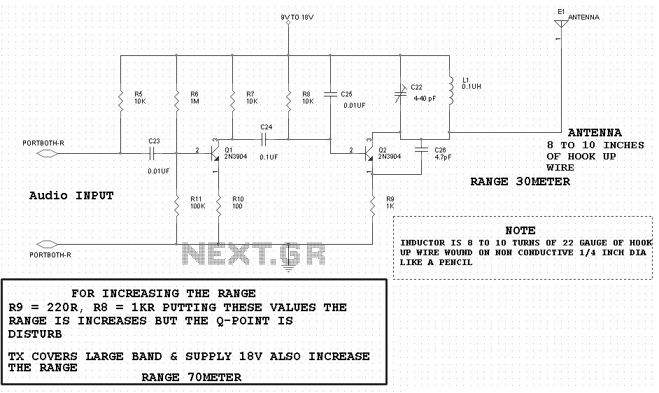
The audio mixer allows for easy comparison of various receivers by adjusting the gain controls without the need for switching. This setup simplifies A/B comparisons since all receivers are connected to the same antenna. Previously, different speakers were used...
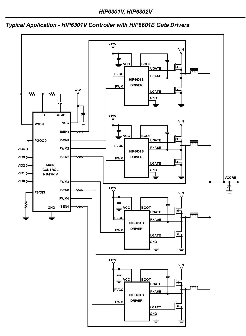
The HIP6301V and HIP6302V control the microprocessor core voltage regulation by driving up to four synchronous-rectified buck channels in parallel. The multiphase buck converter architecture employs interleaved timing to increase ripple frequency and minimize input and output ripple currents....