
Multiple waveform generator circuit diagram

The circuit utilizes a 555 timer IC configured in astable mode, which is essential for generating continuous waveforms. The timing capacitor C2, in conjunction with the resistors R2, R3, and the variable resistor RP, establishes the frequency of oscillation. The relationship between the resistors and capacitor determines the charging and discharging cycles, which are critical for achieving the desired waveform characteristics.
Upon powering the circuit, the 555 timer generates a square wave output at pin 3. The frequency of the square wave can be adjusted by varying the resistance of the potentiometer RP, allowing for a range of output frequencies. The square wave is then passed through an integration network formed by resistor R4 and capacitor C5, which smooths the transitions of the square wave, resulting in a triangular waveform. This triangular waveform is further refined through another integration network comprising resistor R5 and capacitor C6, which approximates a sine wave output.
Capacitor C1 plays a crucial role in stabilizing the power supply by filtering out any noise, ensuring that the 555 timer operates effectively. The inclusion of an LED as a power indicator provides a visual cue to the user that the circuit is functioning properly. Overall, this signal generator circuit is an excellent educational tool for understanding waveform generation and the principles of oscillation in electronic circuits. Circuit is shown at the same time produce a square wave, triangle wave, sine wave and outputs, especially for electronics enthusiasts and students do with an oscilloscope to ob serve the signal waveform of the experiment. The signal generator circuit is simple, low cost, easy adjustment. 555 timer connected as multivibrator forms of work, C2 for the timing capacitor, C2 of the charging circuit is R2 R3 RP C2; C2 discharge circuit is C2 RP R3 IC 7 feet (discharge). Since R3 + RP R2, the charging time constant and the discharging time constant approximately equal to the 3-pin output of the IC is approximately symmetrical square wave.
Press the component parameters as shown in Figure, the frequency is about 1kHz, adjust the potentiometer RP can change the frequency of the oscillator. Square wave signal by R4, after the C5 integration network, the output of the triangular wave. Triangle wave and then by R5, C6 integration network, the approximate sine wave output. C1 is the power supply filter capacitor. Used as a power indicator light-emitting diode VD.
Related Circuits
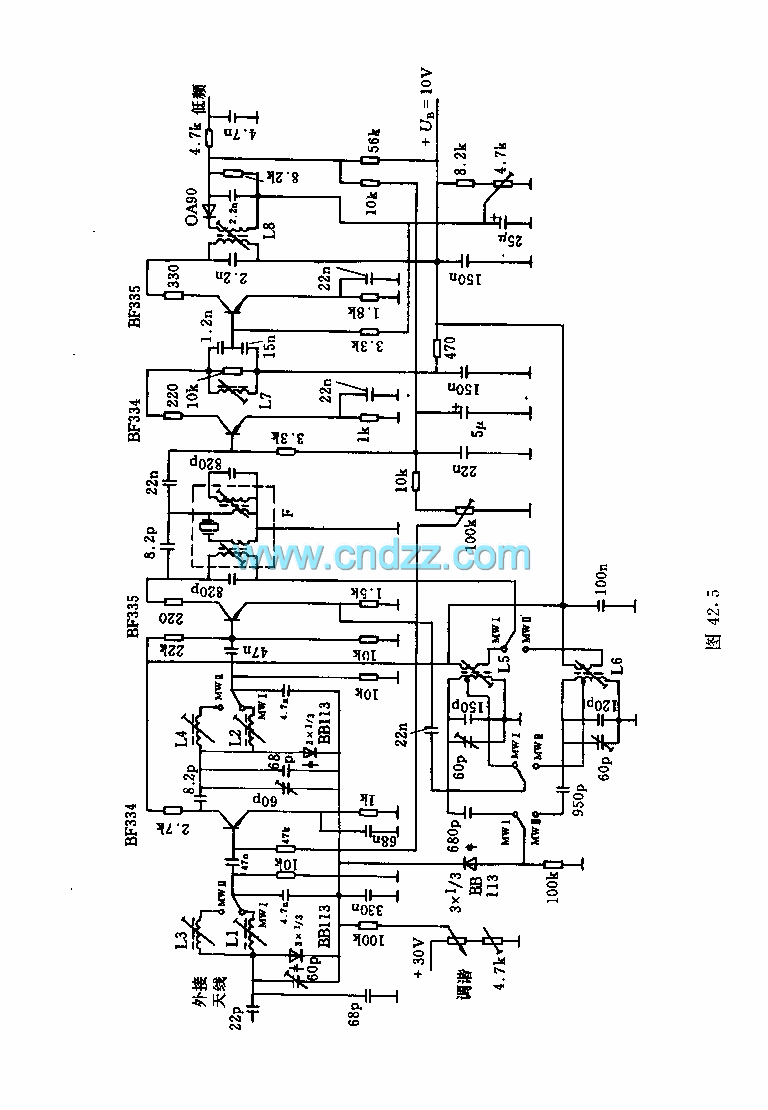
This circuit illustrates the high and mid-frequency sections of a car radio. The medium wave band I operates within the frequency range of 520 to 950 kHz, while Poland II operates between 900 and 1640 kHz. The circuit employs...
It is sufficient to explore PWM (Pulse Width Modulation) and digital-to-analog conversion, illustrating how to create a personal electronics workbench for investigating RC (Resistor-Capacitor) filters, charge and discharge curves, pulse generators, timers, and even a simple oscilloscope to understand...
A low-pass filter is a stable state-space system that has an input and produces an output. If the input is a quasi-periodic signal, the output will be the same quasi-periodic signal with a phase shift. The key difference is...
Figure 4-27 (b) line demonstrates a configuration that enhances the output current waveform DC voltage compared to the line in Figure 4-27 (a). This configuration can be utilized for motors with larger capacities. The circuit illustrated in Figure 4-27 (b)...

As shown in the generator start battery automatic monitor circuit diagram. The generator start battery automatic monitor circuit is designed to oversee the battery's status during generator operation. This circuit ensures that the battery remains charged and functional, preventing premature...
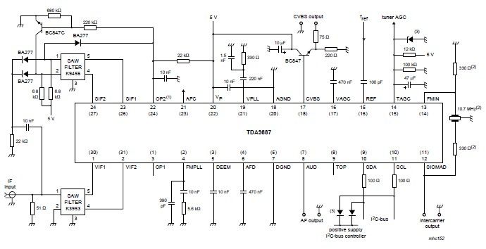
The integrated circuit (IC) is a multistandard vision and sound intermediate frequency (IF) phase-locked loop (PLL) demodulator that operates without the need for alignment. It supports multiple standards, including PAL, SECAM, and NTSC, and is capable of processing both...