
Multivibrator
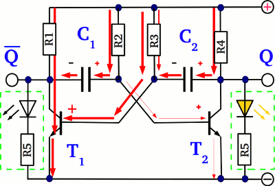
When using a transistor as a switch, the device can be in one of two states: "on," where the voltage drop across the emitter-collector junction is nearly zero, or "off," where the voltage drop across this junction is close to the supply voltage of the circuit. When the left transistor (T1) is turned "on," the base pin of T2 is connected through a series resistor to the collector pin of T1. If T1 is "on," the voltage drop at its emitter-collector junction is nearly zero, resulting in zero voltage at the base pin of T2, which turns T2 "off." Consequently, the voltage drop at the emitter-collector junction of T2 is nearly equal to the supply voltage, providing feedback to the base pin of T1, which allows T1 to remain "on."
The circuit achieves a stable state: while T1 is "on," T2 is "off," and this feedback sustains the "on" state of T1. When T1 is turned "off," the voltage drop at its emitter-collector junction increases to nearly the supply voltage. This change in voltage at the base pin of T2 causes T2 to switch from "off" to "on." Even if switch S is released, the circuit retains its state. The voltage drop at Q approaches the supply voltage, turning the LED at Q "on," while the LED at Q remains "off." Pressing button S again does not change the circuit state since the base pin of T1 is already connected to the emitter-collector junction of T2.
When T2 is "on" and button R is pressed, the base pin of T2 becomes grounded, switching the states of T1 and T2 from "on" to "off" and "off" to "on," respectively. The output Q of the circuit is set by pressing button S and reset by pressing button R. Q serves as the inverting output: when Q is set (voltage output equals the supply voltage), Q is reset (voltage output is zero), and vice versa.
For operation via electric pulses instead of mechanical switches, two resistors (R4 = R2) and two diodes must be added. This modification allows the transistors to be activated by a positive voltage. The diodes prevent the transistors from turning "off" when the input voltage drops to zero. Compared to the previous flip-flop design, the circuit has been slightly adjusted: the coupling resistor at the base of T2 has been replaced with a capacitor, and an additional resistor (denoted as R2) is connected between the supply voltage and the base pin of T2.
In the initial state, T2 is "on," which pulls the base voltage of T1 to ground through the coupling resistor R3, turning T1 "off." The base current of T2 flows from the positive terminal through R2, maintaining the circuit's switching state. The voltage across the capacitor in this stable state is also notable: the left side of the capacitor is connected to the collector pin of T1 (which is "off," thus nearly at the supply voltage VS), while the right side is connected to the base pin of T2 (which is "on," thus receiving approximately 0.7V).
This configuration allows for stable operation of the flip-flop circuit, ensuring that the state can be maintained or changed based on the input signals provided by the push buttons or electric pulses.At one of the previous chapters we have learned how to use a transistor as an electronic switch. At this chapter we will see how a transistor can be used to switch another one. At the drawing you can see a pair of cross coupled transistors. S (set) and R (reset) are the input push buttons of the circuit, while Q and Q are the output clamps. While using a transistor as a switch, the state of the device can be either "on" (the voltage drop at the emitter-collector line is nearly zero) or "off" (the voltage drop at the emitter- collector line equals nearly the supply voltage of the circuit). So what happens, if the left transistor (T1) is turned "on" The base pin of T2 is connected via a series resistor to the collector pin of T1, so if the voltage drop at the emitter-collector line of T1 is (nearly) zero, the voltage drop at the base pin of T2 and so the current running through those pin is also zero, hence T2 is turned "off".
While the voltage drop at the emitter-collector line of T2 equals (nearly) the supply voltage, the voltage feedback passed to the base pin of T1 and so the current running through the base of T1 is at it`s maximum, causing T1 to be turned "on". So the state of the circuit is stable: While T1 is turned "on", T2 gets turned "off", providing a feedback voltage which sustains the switching state of T1 ("on").
The current running through the base pin of T1 prior to this is now cut off, because the emitter base line of the transistor is shortened. Consequently T1 is turned "off", which is why the voltage drop at the emitter collector line increases to nearly the supply voltage.
The voltage feedback passed to the base pin of T2 causes the right transistor to alter it`s state from "off" to "on". Now that T2 is turned "on", the feedback passed back to the base of T1 is zero. Even if the switch S is released, the circuit retains the switching state. Now the voltage drop at Q is nearly the supply voltage, while those at Q is nearly zero. The LED at Q is turned on, those at Q is turned off. Pushing button S once again doesn`t alter the state of the whole circuit, because the base pin of T1 is already shortened by the emitter-collector line of T2.
While T2 is turned "on" and button R is pushed, the base pin of T2 gets shortened, altering the switching state of those transistor from "on" to "off" which in turn alters the switching state of T1 from "off" to "on". By pushing the S button, the output Q of the circuit is set, while it is reset by pushing the R button.
Q is the inverting output of the circuit: Whenever Q is set (the voltage output equals the supply voltage), Q is reset (the voltage output is zero) and vice versa. If your intention is to operate the flip-flop by electric pulses instead of mechanical switches, two resistors (R4 = R2) and two diodes have to be inserted.
Now the transistors are turned "on" by a positive voltage. Because of the diodes, the transistors are not turned "off" if the input voltage drops to zero. In comparison to the flip-flop drawn above, the circuit is now altered slightly: The coupling resistor at the base of T2 has been replaced by a capacitor and an additional resistor is connected between the terminal of the supply voltage and the base pin of T2 (here denoted as R2). At the initial state, T2 is turned "on", pulling the base voltage of T1 to ground via the coupling resistor R3, hence T1 is turned "off".
The base current of T2 is running from the positive terminal via R2, retaining the switching state of the circuit. What about the voltage across the capacitor at this stable state of the circuit The left side of the capacitor is connected to the collector pin of T1, which is turned "off", hence the potential at those pin equals nearly the supply voltage VS.
The right side of the capacitor is connected to the base pin of T2 which is turned "on", hence a potential of approximately 0. 7V is applied to those pin (see prope 🔗 External reference
Related Circuits
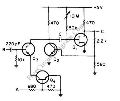
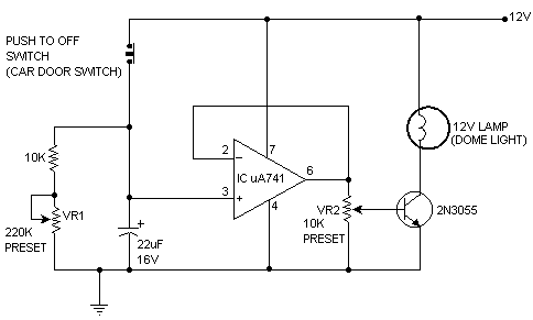
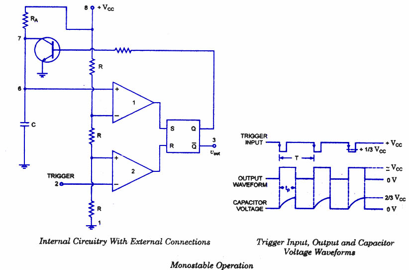
This is a versatile discrete monostable circuit. The circuit consists of a 2N3819 JFET and 2N3704 transistors. This monostable multivibrator circuit has an additional input to enable or inhibit the function at any time without causing an output pulse....
Function: to trigger a device or operate in free-running mode. Components: Battery, Charger, Battery Connector, Capacitor, Integrated Circuit (IC), Resistor VR1-10K, Resistor R1-1K, Resistor R2. The described circuit functions either to trigger a connected device or to operate in a...
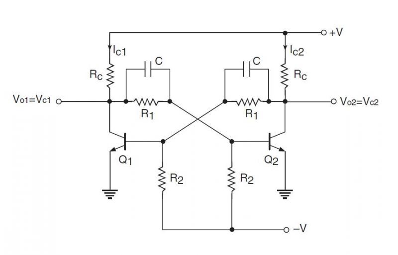
Multivibrators, unlike sinusoidal oscillators, are circuits with regenerative feedback that produce pulsed outputs. There are three primary types of multivibrators: the Bistable Multivibrator, the Monostable Multivibrator, and the Astable Multivibrator. A bistable multivibrator circuit maintains stable LOW and HIGH...
The circuit utilizes a CMOS dual D flip-flop (CD4013) to toggle a relay or other load using a momentary push button. Multiple push buttons can be connected in parallel to control the relay from different locations. A high signal...
Are you familiar with the basics and applications of the 555 timer IC? Are you looking for a book that provides all these basics? If so, CircuitsToday has started an online store where you can purchase books on the...
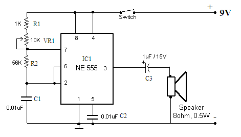
The objective is to design a square-wave generator with an output range of 0 to +5V. Additionally, the design should allow for the modification of the signal to enable adjustment of the duty cycle of the pulse (PWM). The square-wave...