
MW0LLO RF Milliwatt Meter
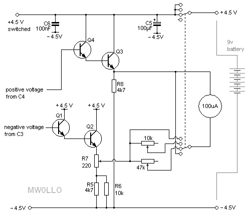
The RF power meter circuit is composed of two main sections: the RF detection section and the DC measurement section. The RF detection section utilizes a dummy load formed by resistor R1, which receives the RF input signal. Capacitor C1 serves as a DC blocking capacitor, allowing RF signals to pass while preventing DC voltage from affecting the measurement. The use of diodes D1 and D2 enables the circuit to rectify the RF signal, capturing both the peak positive and peak negative voltages. This rectification process is essential for accurately measuring the RF power.
To enhance the accuracy of the diode rectification, a small DC bias current is introduced into the system. This bias current, flowing through resistors R4 and Rx, ensures that the diodes operate in their linear region, thus improving measurement accuracy at low power levels. The configuration of the power supply, with +4.5V and -4.5V lines, provides the necessary voltage levels for proper operation of the circuit while maintaining a common reference point for both the RF and DC sections.
The DC measurement section is designed to analyze the rectified voltages across capacitors C3 and C4, allowing for the determination of the RF power based on the difference between the peak voltages. The Darlington pair configuration used in the original design offers high input impedance, which is crucial for minimizing the loading effect on the RF signal being measured. This configuration allows for accurate voltage measurement without significantly affecting the circuit's performance.
Overall, this RF power meter circuit is a valuable tool for accurately measuring low RF power levels, particularly in applications where sine wave signals are prevalent. By addressing the limitations of traditional RF power meters, this design provides enhanced accuracy and reliability for RF measurements in various electronic applications.This project, based on an article published in the February 2008 edition of Radcom (the magazine of the Radio Society of Great Britain) is for a meter with a 50 ohm input impedance for measuring very small RF powers. Many RF power meters become inaccurate at low powers, but this meter is able to measure down to very low levels.
From a theoretical standpoint, the meter is only able to accurately measure the power of steady, sine wave voltage RF - it would not be suitable for square wave signals for example. In practice, however, the most common requirement is to measure the power of sine wave signals and to compare power readings (when peaking up IF stages, for example).
The reason that the meter is best suited to sine waves is that the circuit actually measures the peak-to-peak voltage in order to infer the power. The Radcom article explains how many RF `sniffer` type projects rely on detecting RF using a diode. This diode will require a certain amount of voltage to bring it into forward conduction, and this is the source of inaccuracy at low powers for more conventional designs.
The original article gives details for a meter based on PNP transistors. I am more used to understanding circuits based on NPN transistors, so I first redrew the circuit diagram with NPN transistors and the diodes and PSU reversed. Once I had a good understanding, I realised that the design can be broken down into two sections; I call these the RF section and the DC voltmeter section.
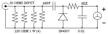
The RF part of the circuit is basically a dummy load with two detecting diodes to get the peak positive and peak negative voltages. A DC blocking capacitor is connected at the input, which acts as a short circuit at RF frequencies. What makes this design different is that the detecting diodes are driven into conduction by a small dc current.
In the circuit diagram from the original article, the power supply (a 9V battery) is shown as a 0V earth and a +9V supply line, and a +4. 5V reference is derived for the earth of the RF section. To make the understanding of the RF section easier, however, I have chosen to show this as a 0V RF and DC earth, with +4.
5V and -4. 5V supply lines. The difference is academic. The circuit diagram is shown below: The input signal passes through C1 and into the dummy load formed by R1. The diodes D1 and D2 then rectify the negative and positive peaks respectively of the signal across R1.
The rectified voltages appear across C3 and C4, minus the forward voltage drop of the diodes. To bring the diodes into conduction and improve linearity, a small DC current of a little under 0. 5 µA passes from the +4. 5V supply line, through R4, D1, D2 and Rx to the -4. 5V supply line. Note that in the Radcom article, Rx was not used and instead the current flowed into the DC measuring circuit input impedance. The DC blocking capacitor C1 will have a reactance of about 1. 6 ohms at 1MHz, so this device will give less accurate results below 1MHz unless the value of C1 is increased.
This part of the circuit measures the difference between the peak negative and peak positive voltages. The original circuit had two halves, each consisting of two transistors connected in a Darlington confiuration, to give an emitter follower of high input impedance.
As the emitter followers are referenced to the negative supply line, this gives no problem in measuring the peak negative voltage of the input RF. Note: Some pages of this web site contain mathematical formulas presented using Presentation MathML (links to and the MathJax (links to JavaScript software.
The formulas may also be presented in plain text and or as an image in case your particular web browser does not render the formulas correctly. 🔗 External reference
Related Circuits
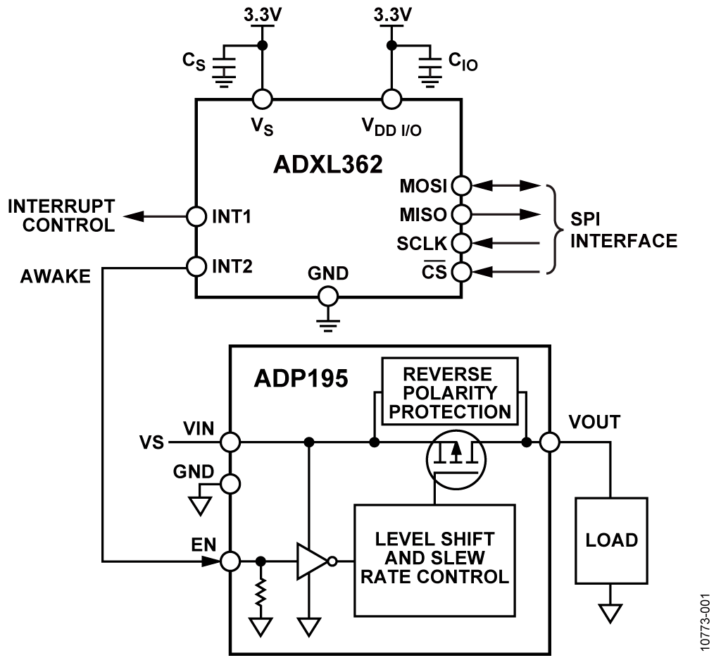
The ADXL362 is an ultra-low power, 3-axis MEMS accelerometer that consumes less than 2 µA at a 100 Hz output data rate and 270 nA when in motion-triggered wake-up mode. Unlike accelerometers that utilize power duty cycling to achieve...
Power input is to a 7805 5 volt regulator. A pair of LEDs is connected between the 5 volt supply and ground, with current limiting resistors in series and one pin on the AT90S2313 shunts the current through one...
This circuit utilizes a probe that contains a Clairex 905HN light-dependent resistance element, which is connected to a DC differential amplifier. The amplifier drives a meter with a specially calibrated scale. The article outlines the calibration procedure. A switching...
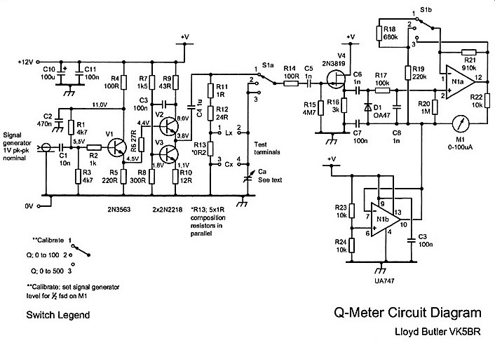
The Q meter has been an essential piece of equipment for laboratories engaged in the testing of radio frequency circuits. In modern laboratories, the Q meter has been largely replaced by more advanced and costly impedance measuring devices, making...
Many beginners trying out their skill with QRP TX for the first time have to overcome many problems before they are able to come on the air. One usual complaint is that everything is working fine, but the signal...
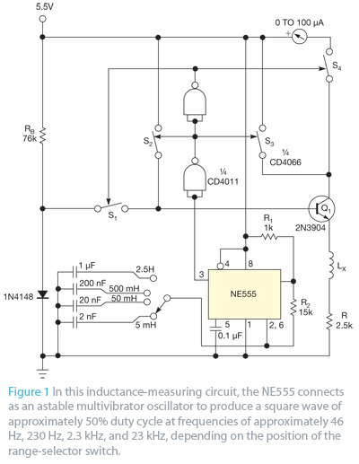
Bipolar junction transistors transfer a current from a lower-resistance emitter to a higher-resistance collector. This property can be utilized to measure inductance. Bipolar junction transistors (BJTs) are semiconductor devices that play a crucial role in electronic circuits by enabling the...