
NAND gate S-R flip-flop
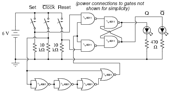
The circuit described involves a ten-segment LED display or two individual LEDs, which function as visual indicators for the output states of the flip-flop. The flip-flop is designed using a combination of NOR gates configured to create a pulse detector that converts a gated latch into a flip-flop. The pulse detector's role is crucial, as it ensures that the flip-flop responds correctly to clock signals by generating a brief high pulse at the falling edge of the clock, which allows for accurate transitions between Set and Reset states.
The use of a 4001 integrated circuit is significant, as it contains four NOR gates, which are versatile components in digital logic design. The intentional design choice to parallel the inputs of the NOR gates to create inverters is a deviation from standard practice, which typically emphasizes speed. In this scenario, the slower response time is leveraged to mitigate the effects of contact bounce, allowing for a more stable operation of the flip-flop circuit.
The circuit's response to the mechanical switch's bounce is a critical consideration in its design. The mechanical switch's inherent imperfections can lead to unintended triggering of the flip-flop, which necessitates careful attention in practical implementations. This understanding of contact bounce and its implications on circuit behavior is essential for engineers and designers working with digital systems. Proper debouncing techniques or circuitry may be employed to ensure that the flip-flop operates reliably, responding only to intended state changes rather than erratic signals caused by mechanical imperfections.Although the parts list calls for a ten-segment LED unit, the illustration shows two individual LEDs being used instead. This is due to lack of room on my breadboard to mount the switch assembly, two integrated circuits, and the bargraph.
If you have room on your breadboard, feel free to use the bargraph as called for in the parts list, and as sho wn in prior latch circuits. The only difference between a gated (or enabled) latch and a flip-flop is that a flip-flop is enabled only on the rising or falling edge of a "clock" signal, rather than for the entire duration of a "high" enable signal. Converting an enabled latch into a flip-flop simply requires that a "pulse detector" circuit be added to the Enable input, so that the edge of a clock pulse generates a brief "high" Enable pulse: The single NOR gate and three inverter gates create this effect by exploiting the propagation delay time of multiple, cascaded gates.
In this experiment, I use three NOR gates with paralleled inputs to create three inverters, thus using all four NOR gates of a 4001 integrated circuit: Normally, when using a NOR gate as an inverter, one input would be grounded while the other acts as the inverter input, to minimize input capacitance and increase speed. Here, however, slow response is desired, and so I parallel the NOR inputs to make inverters rather than use the more conventional method.
Please note that this particular pulse detector circuit produces a "high" output pulse at every falling edge of the clock (input) signal. This means that the flip-flop circuit should be responsive to the Set and Reset input states only when the middle switch is moved from "on" to "off, " not from "off" to "on.
" When you build this circuit, though, you may discover that the outputs respond to Set and Reset input signals during both transitions of the Clock input, not just when it is switched from a "high" state to a "low" state. The reason for this is contact bounce: the effect of a mechanical switch rapidly making-and-breaking when its contacts are first closed, due to the elastic collision of the metal contact pads.
Instead of the Clock switch producing a single, clean low-to-high signal transition when closed, there will most likely be several low-high-low "cycles" as the contact pads "bounce" upon off-to-on actuation. The first high-to-low transition caused by bouncing will trigger the pulse detector circuit, enabling the S-R latch for that moment in time, making it responsive to the Set and Reset inputs.
Ideally, of course, switches are perfect and bounce-free. In the real world, though, contact bounce is a very common problem for digital gate circuits operated by switch inputs, and must be understood well if it is to be overcome. 🔗 External reference
Related Circuits
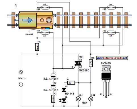
Modern electronics is essential for every large model railroad system, providing solutions to nearly every issue. Although ready-made products are available... Modern model railroad systems rely heavily on advanced electronics to enhance functionality and user experience. These systems often incorporate...
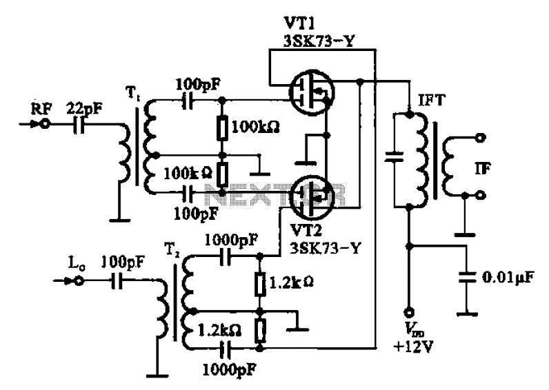
A balanced mixer circuit is illustrated using two dual-gate field effect transistors (FETs). The RF signal is coupled to the gates of these transistors through an input signal transformer (T1). Additionally, a local oscillation signal is introduced to the...
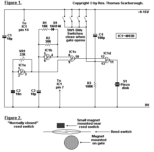
The circuit utilizes reed switches to create a gate alarm that is powered by a universal AC/DC power supply oscillator. The design of this gate alarm circuit incorporates reed switches, which are electromechanical devices that operate based on the presence...
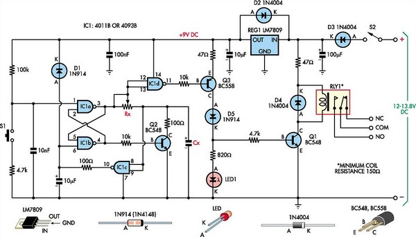
This timing circuit is designed to time one-shot events ranging from a few seconds to several hours. In standby mode, with RLY1 and LED1 turned off, the power consumption is minimal. The main component of this circuit is a...
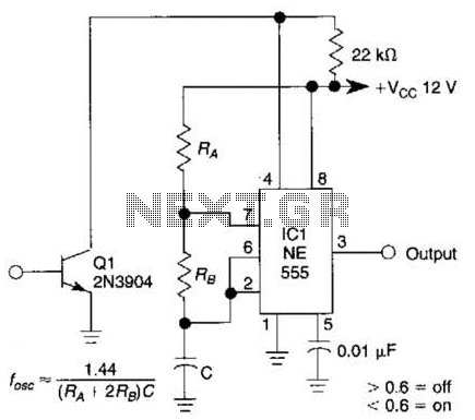
This gated 1-kHz oscillator provides press-to-turn-off functionality, along with waveforms available at the output of pin 3 and across capacitor C1. The gated 1-kHz oscillator circuit is designed to generate a square wave output at a frequency of 1 kHz....
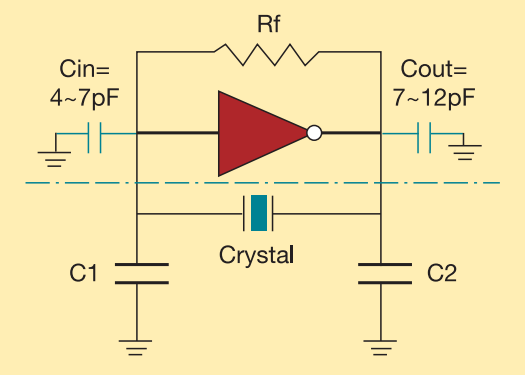
The crystal used in the topology of Figure 1 can be either a fundamental AT-CUT or BT-CUT. A BT-CUT crystal has poor frequency stability over temperature compared to an AT-CUT. This topology uses a parallel crystal and not a...