
Negative Voltage Generator Schematic
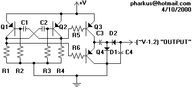
This circuit starts with a single-polarity (GND and +V) input and produces an approximate opposite voltage (-V), enabling dual-polarity op amp circuits to be used with single-polarity supplies.
Theory of Operation: This circuit is designed to power a microphone preamp from an unregulated, noisy, single-polarity 12V supply that also powers other devices. The circuit employs a multivibrator configuration using transistors Q1 and Q2, along with capacitors C1 and C2, and resistors R1 through R4. The multivibrator generates oscillating signals that drive transistors Q3 and Q4, which act as current amplifiers.
When Q3 is activated, it connects the positive voltage (+V) to capacitor C3, allowing it to charge. Once C3 is charged, Q3 deactivates and Q4 is activated, connecting the negative terminal of C3 to ground. This results in C3's negative terminal being at a voltage level that is below ground, effectively producing a negative voltage output. The output voltage is taken through diode D2. Capacitor C4 acts as a filter capacitor for the negative voltage, providing current during the charging cycles of C3, ensuring a stable output voltage.
The component values are as follows:
- Resistors: R1 = 1K, R2 = 10K, R3 = 10K, R4 = 1K, R5 = 1K, R6 = 1K
- Capacitors: C1 = 0.1µF, C2 = 0.1µF, C3 = 1000µF, C4 = 1000µF
- Transistors: All transistors are 2N3906 General Purpose PNP types.
- Diodes: Generic silicon rectifiers are used.
This configuration provides a practical solution for applications requiring dual-polarity power supplies from single-polarity sources, while also highlighting potential noise issues inherent in the design.Most operational amplifier circuits require a dual-polarity power supply - one having +V and -V. However, there are times when a DP supply simply isn't conveniently available. Single-polarity modifications to DP designs often acheive their effect by referencing the input to a "synthetic ground", derived using a resistive voltage divider. This renders the resulting circuit highly sensitive to power supply noise, since any variation in the power supply will be divided by the divider, then used as an input reference, and amplified by the circuit in question.
While this is of little concern with battery sources, AC "wall-warts" and many DIY power supplies are chock full of horrendous 60Hz buzz that is sure to get into the circuit. By powering an op amp with a dual-polarity supply, we are able to reference all signals to a definite solid 0V ground. This circuit starts with a single-polarity (GND and +V) input and produces an approximate opposite voltage (-V), enabling dual-polarity op amp circuits to be used with single-polarity supplies.
Theory of Operation This circuit was built in a pinch because I needed to power a microphone preamp from an unregulated, noisy, single-polarity 12V supply that also powers a couple of power-hungry sirens and a video camera. While said preamp is now working relatively successfully, this circuit is a quick design that has not been put through extensive testing.
I do not know its current limitations. Some components on the board can be heard to be "whining", much like a switchmode power supply. This does not indicate a problem, as none of the components run particularly hot. Also like a SMPS, this noise is slightly detectable on the output. Q1, Q2, C1, C2, R1, R2, R3, and R4 form a multivibrator -- an oscillator. We are using both of its outputs which are opposites of one another: when one is on, the other is off. These outputs go through R5 and R6 to turn on Q3 and Q4 - one at a time, of course. This applies a wave oscillating from +V to GND to C3. This is where things get interesting. Q3 and Q4 form a current amplifier. When Q3 is turned on, +V is applied to C3. We can envision the current going through C3 and D1 to ground. This charges C3. Next, Q3 turns off and Q4 turns on, applying GND to C3. C3's + terminal is now at GND. Since C3 is charged to nV, its - terminal has to be n volts below its + terminal, meaning that its - terminal is n volts below GND.
This goes through D2 and is our output. C4 is a filter capacitor for -V, and serves up the current filling in the gaps when C3 is charging. R1 1K R2 10K R3 10K R4 1K R5 1K R6 1K Capacitors C1 .1uF C2 .1uF C3 1,000uF C4 1,000uF All transistors: 2N3906 General Purpose PNP All diodes: Generic silicon rectifiers 🔗 External reference
Related Circuits
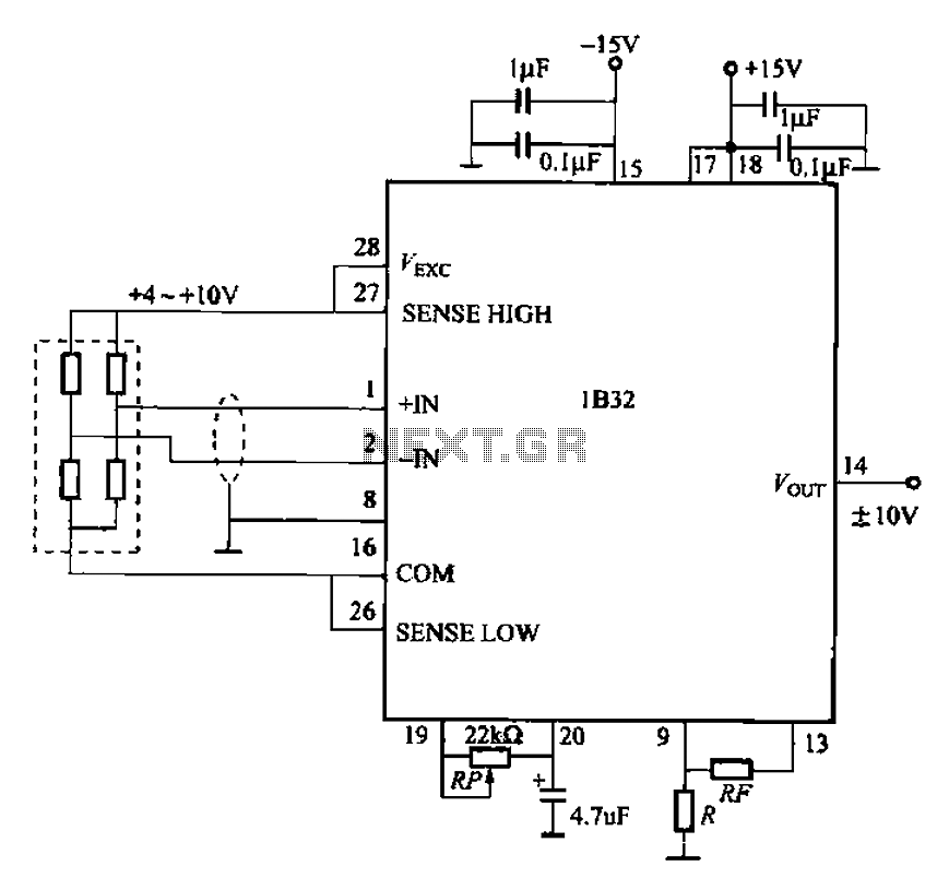
The circuit for bridge measurements is straightforward, as illustrated in the figure. The sensor bridge drive voltage can be adjusted between +4V and +10V, depending on the specific requirements of the sensor. Two fixed gain options of 333.3 and...
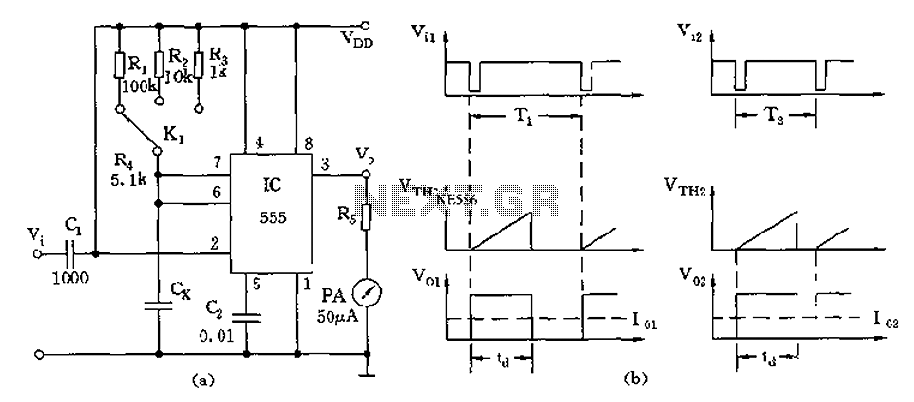
The circuit utilizes a 555 timer along with timing resistors R1 to R3 and a measured capacitance Cx to create a capacitance meter. The principle of capacitance measurement in a one-shot circuit is based on the relationship between the...
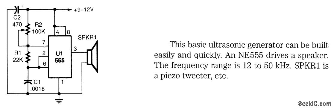
This basic ultrasonic generator can be built easily and quickly. An NE555 drives a speaker. The frequency range is 12 to 50 kHz. SPKRI is a piezo tweeter. The ultrasonic generator circuit utilizes the NE555 timer integrated circuit, which is...
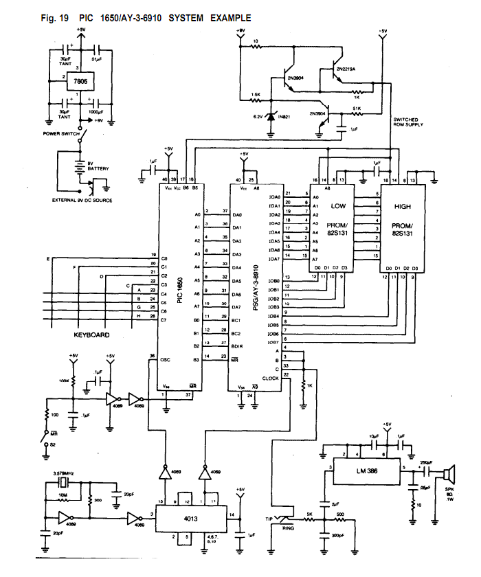
The AY-3-8910/8912 is a register oriented Programmable Sound Generator (PSG). Communication between the processor and the PSG is based on the concept of memory-mapped I/O. Control commands are issued to the PSG by writing to 16 memory-mapped registers. Each...
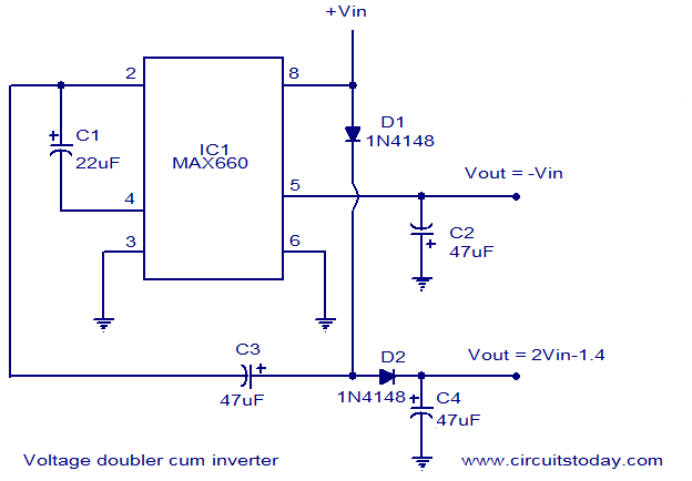
Voltage doubler circuit and voltage inverter circuit diagram with schematics using MAX660 IC, which is a DC voltage multiplier IC. This is a DC voltage doubler circuit and inverter. The MAX660 integrated circuit (IC) is designed for applications requiring a...
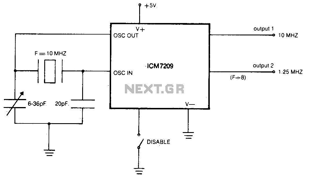
The CMOS IC directly drives five TTL loads from either of two buffered outputs. The device operates at up to 10 MHz and is compatible with bipolar, MOS, and CMOS technologies. The CMOS integrated circuit (IC) is designed to interface...
Warning: include(partials/cookie-banner.php): Failed to open stream: Permission denied in /var/www/html/nextgr/view-circuit.php on line 713
Warning: include(): Failed opening 'partials/cookie-banner.php' for inclusion (include_path='.:/usr/share/php') in /var/www/html/nextgr/view-circuit.php on line 713