
NFC Tag communication system

The circuit design involves calculating the resonance capacity using a specific formula, which is essential for optimizing the performance of the NFC (Near Field Communication) system. The NFC Tag LSI, or Large Scale Integration, is a critical component that facilitates communication between the NFC tag and the reader.
The antenna circuit board is designed to support the NFC Tag LSI, ensuring that it can effectively transmit and receive signals. The resonance frequency of the antenna is a crucial parameter that affects the efficiency of the NFC communication. This frequency must be precisely measured to ensure that the antenna operates at its optimal performance level.
After measuring the resonance frequency, adjustments to the resonance capacity are necessary. This adjustment process may involve changing the values of capacitors in the circuit or altering the physical dimensions of the antenna to achieve the desired resonance frequency.
The overall goal of this process is to ensure that the NFC system operates reliably and efficiently, facilitating seamless communication in applications such as mobile payments, access control, and data transfer. Proper tuning of the resonance capacity directly impacts the range and effectiveness of the NFC communication, making it a vital aspect of the circuit design.A calculating resonance capacity from formula (1) and NFC Tag LSI are set to antenna circuit board, and measured resonance frequency, after that, adjusting resonance capacity 🔗 External reference
Related Circuits
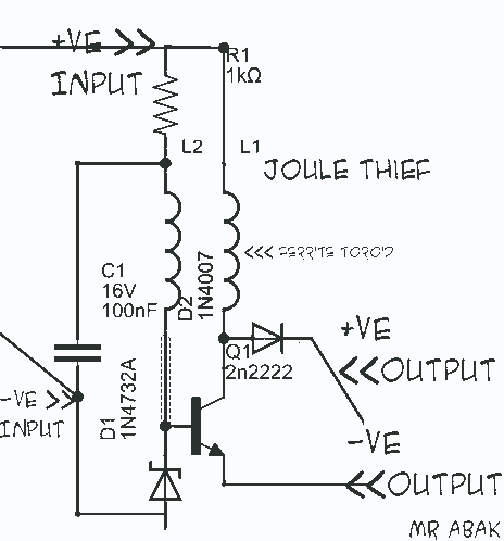
This circuit diagram is provided for those interested. It is a small circuit that takes an input of 1.5 volts and outputs 120 volts. The circuit in question is a voltage step-up converter, commonly referred to as a boost converter....
The ICM7226 is a fully integrated Universal Counter and LED Display driver. It combines a high-frequency oscillator, a decade timebase counter, an 8-decade data counter and latches, a 7-segment decoder, digit multiplexer, and segment and digit drivers, which can...

The mobile robot is designed to operate in unknown and uncertain environments, featuring autopilot capabilities while avoiding obstacles. It utilizes ultrasonic sensors for range finding due to their simplicity, speed, and cost-effectiveness in information processing. These sensors facilitate functions...
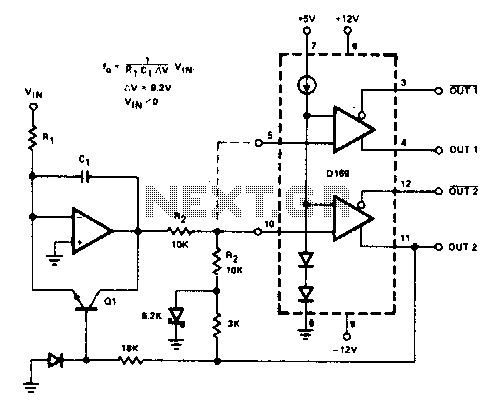
The D169 functions as a level detector, offering complementary outputs. An operational amplifier (op amp) is employed to integrate the input signal Vin, utilizing a time constant defined by the resistor R1 and capacitor C1. A negative input signal...
High-voltage power supply circuit for fluorescent light power supply. Refer to that page for an explanation of the related circuit diagram. The high-voltage power supply circuit designed for fluorescent lights typically consists of several key components that work together to...
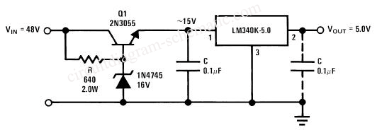
This circuit is a high input voltage regulator that generates a voltage of 5V. In this circuit, the input voltage for the LM340 must remain within the limits specified in the datasheet. Operating the device above the absolute maximum...