
Noise limiter
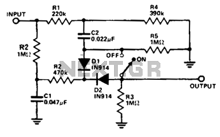
The limiter circuit operates by controlling the amplitude of the signal passing through it, effectively reducing the noise level while preserving the integrity of the desired audio signals. The placement of the limiter is crucial; it should be positioned between the output of the detector and the input of the audio stage to ensure optimal performance. The high-impedance nature of the connection helps to prevent loading effects that could distort the audio signal.
In this configuration, diodes D1 and D2 play a significant role. Their low forward resistance allows them to conduct when the signal exceeds a certain threshold, effectively clamping the signal to prevent it from exceeding this limit. The high reverse resistance ensures that the diodes do not conduct during negative cycles of the audio signal, thereby maintaining the integrity of the audio waveform.
The choice of capacitor C1 is also critical. Increasing its value will allow the circuit to function effectively with receivers that have narrower bandwidths, which typically require better signal conditioning to minimize distortion and maintain clarity. The overall design of this limiter circuit is tailored to enhance the performance of audio receivers, particularly in environments where signal-to-noise ratios are a concern, ensuring that the output maintains a high level of fidelity despite the presence of noise.This limiter improves signal-to-noise ratio. It is connected between the detector output and the audio input (if high impedance) or at some relatively high-impedance section between two audio stages—preferably the low level stages.D1 and D2 can be any diode having relatively low forward resistance and very high back resistance. The circuit is excellent for receivers having bandwidths down to 2 or 3 kHz. Increase the value of Cl for receivers having narrower bandwidths. 🔗 External reference
Related Circuits
When a transistor junction operates in Zener breakdown as a noise source, the resulting noise signal exhibits asymmetry in amplitude. This issue can be addressed by employing two transistors as independent noise sources. One transistor is connected with a...
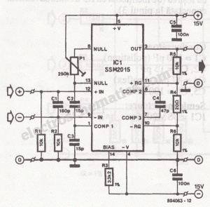
The microphone preamplifier circuit design presented in this schematic utilizes the SSM2015 produced by Precision Monolithics Inc. (PMI), which offers high amplification. The SSM2015 is a low-noise, low-distortion integrated circuit designed specifically for microphone preamplification. It features a differential input...
A preamp circuit in a powered subwoofer is producing a static or popping noise, reminiscent of a scratchy or dirty sound. The preamp circuit in question is crucial for amplifying low-level audio signals before they are sent to the power...
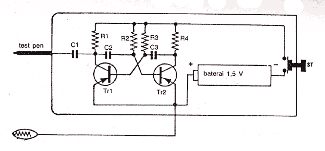
Audio Jammer Noise generator for detector audio circuit More: Parts: R1,R4 . 1K 0,5W R2,R3 . 39K 0,5W C1 . 5000pF/50V C2,C3 . 3000pF/50V FCS9012 . PNP FCS9012 . PNP The audio jammer circuit functions as a noise generator, designed...
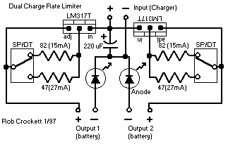
Here is a deluxe version of the simple charge rate limiter, using the same idea but with the ability to charge two packs simultaneously from a single wall charger. For circuit description and parts list, see the simple charger...
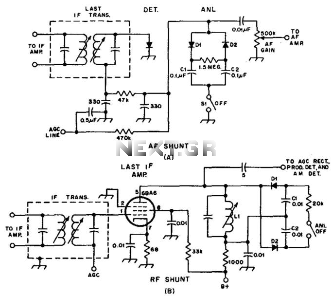
Examples of RF and audio ANL circuits. Positive and negative clipping occurs in both circuits. The circuit is self-adjusting. This noise limiter operates at the IF output. Adequate gain is needed at the IF frequency so that several volts...