
Symmetric Noise Source
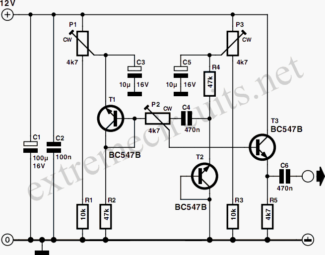
The described circuit effectively utilizes two transistors operating in Zener breakdown mode to generate noise signals that compensate for each other's asymmetries. By strategically placing resistors and capacitors, the circuit not only optimizes the noise generation but also ensures that the output signal is balanced and symmetric. The adjustable voltage supply allows for fine-tuning of the noise characteristics, which is vital for applications requiring precise noise levels. The inclusion of a buffer stage is crucial, as it prevents loading effects that could distort the noise signals when interfacing with subsequent circuitry. The use of an oscilloscope for real-time adjustments enhances the accuracy of the setup, allowing for immediate visual feedback on the noise characteristics. This design is particularly useful in applications such as testing, signal processing, and noise analysis, where controlled noise generation is essential. The careful selection of component values and configurations ensures reliable operation and optimal performance of the noise generator circuit.If a transistor junction operating in Zener breakdown is used as a noise source, the amplitude of the noise signal is asymmetric. This problem can be solved by using two transistors as two independent noise sources. One of these has a series resistor to earth, and the other has a series resistor to the supply line. Each of these noise sources prod uces an asymmetric noise voltage, with opposite asymmetry. If these two voltages are combined, the amplitude of the result will be symmetric. In the circuit diagram, T1 and T2 are the noise sources. The series resistors are R2 (to earth) and R4 (to the positive supply line). The supply voltage for the noise sources has been made adjustable, to allow the noise generation of the transistors to be optimized. This is because the amount of noise produced depends on the power supply voltage. P1 and R1 provide an adjustable supply voltage between 8 and 12 V for the noise stage around T1, while P3 and R3 perform the same function for T2.
C3 and C5 smooth these voltages. Since the amplitudes of the two noise sources will never be the same, it is necessary to take a weighted sum of the two signals. Consequently, P2 is included between the outputs of the noise sources as a sort of balance control. Since the DC levels of the two noise sources are not the same, C4 is also included in the balance network.
The weighted sum of the two signals is present on the wiper of P2, superimposed on the DC signal of noise source T1. This DC level is also used for the DC bias of the buffer stage T3. The buffer isolates the noise sources from whatever circuit is connected to the output. To adjust the circuit, connect an oscilloscope to the output. First, turn P2 all the way to the left. Now rotate P1 until a maximum noise signal is seen on the oscilloscope. Next, turn P2 all the way to the right, and then adjust P3 for the best noise signal. Finally, adjust P3 so that the noise signal looks symmetric. The circuit provides an output voltage of approximately 150mV pp. The current consumption is 2mA. The oscilloscope shows the asymmetric noise signal on channel 2, and the symmetric noise signal on channel 1.
🔗 External reference
Related Circuits
In audio systems, noise signals are generally undesirable, and efforts are often made to eliminate them. Transistors can be utilized effectively for this purpose due to their availability and low noise characteristics. The following circuit serves as a Noise...
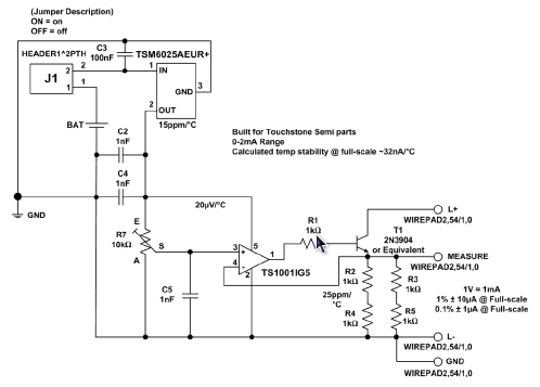
The MicroCC utilizes the Touchstone Semiconductor TSM6025 voltage reference, which serves as a direct replacement for the MAX6025, offering stability of better than 15 ppm/°C. The TSM6025 voltage reference is designed to provide a precise and stable output voltage, making...
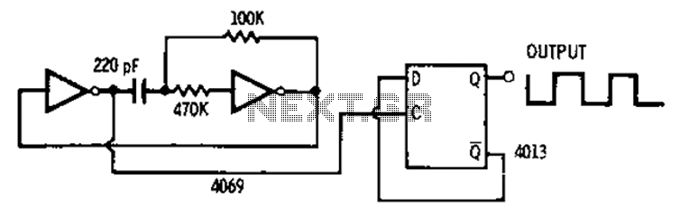
The 4013 pairs of D-type flip-flops in the astable multivibrator configuration are utilized as a binary divider output, generating an output frequency that is symmetrical, with a duty cycle of 50%. The 4013 integrated circuit contains two D-type flip-flops that...
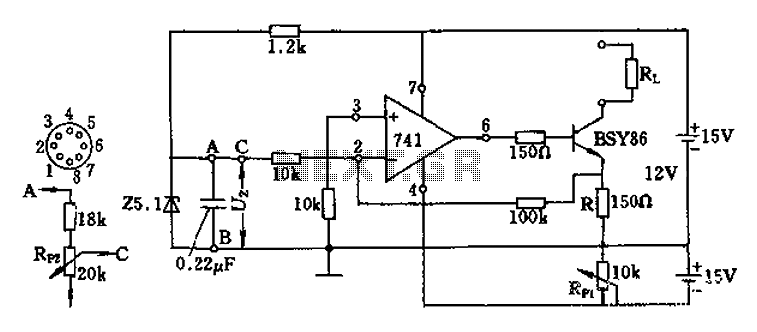
The Darlington transistor circuit BSY86 produces a large output current, with a maximum limit of 150 ohms. The output current is adjustable via resistor R and the RP1 potentiometer, maintaining constancy regardless of the load resistance Rl. The potentiometer...
This low noise audio power supply circuit can reduce noise and ripple voltage by 40 dB over the 100 Hz to 20 kHz audio range. In portable applications such as... This low noise audio power supply circuit is designed to...
This limiter enhances the signal-to-noise ratio. It connects between the detector output and the audio input (if high impedance) or at a relatively high-impedance section between two audio stages, preferably in the low-level stages. Diodes D1 and D2 can...