
Norton high voltage inverting amplifier
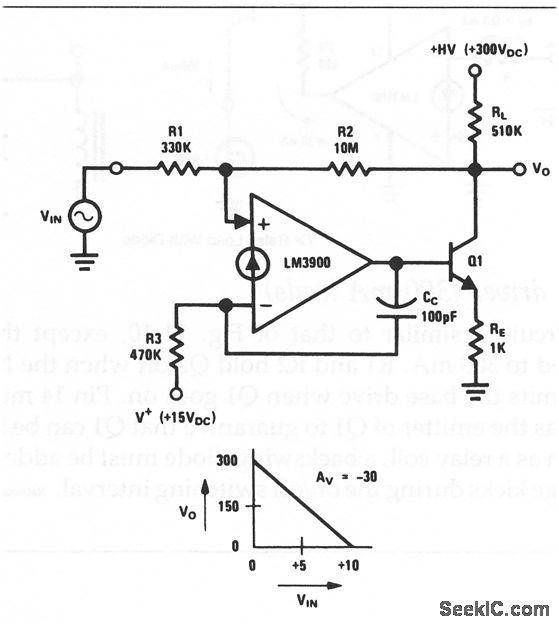
This circuit operates as a high-voltage inverting amplifier, capable of providing a significant voltage swing, which is essential in applications requiring precise control over high voltage outputs. The choice of transistor Q1 is critical; it must be rated for a breakdown voltage greater than 300 V to ensure reliable operation under the specified conditions. Suitable transistor options include high-voltage MOSFETs or BJTs that are capable of handling the required voltage levels without entering breakdown.
The gain of the amplifier is established by the resistor network formed by R1 and R2. Specifically, the gain can be expressed mathematically as -R2/R1, indicating that the output signal will be inverted in phase relative to the input. This negative gain is characteristic of inverting amplifiers, which can be advantageous in signal processing applications where phase inversion is required.
The biasing resistor R3 plays a vital role in stabilizing the amplifier's operation by centering the transfer characteristic, thus ensuring that the output remains linear over the desired range of input voltages. Proper selection of R3 is essential to maintain the desired operating point and minimize distortion in the output signal.
The load resistor RL can be adjusted to manage the current drain from the high-voltage supply. Increasing RL will reduce the current drawn from the power source, which can be beneficial in applications where power efficiency is a concern. However, care must be taken to ensure that the load does not exceed the output capability of the amplifier, which could lead to distortion or clipping of the output signal.
Overall, this inverting amplifier circuit is suitable for high-voltage applications where precise voltage control and efficient power management are required, making it a valuable component in a variety of electronic systems.This circuit is an inverting amplifier with an output voltage swing from essentially 0 to +300 V. Any transistor can be used for Q1, provided that the breakdown voltage is greater than 300 V (because the full high voltage will be applied across Q1). Biasing resistor R3 is used to center the transfer characteristic, and the gain is set by the ratio of R2/R1. Load RL can be increased to reduce the high-voltage current drain, if desired. 🔗 External reference
Related Circuits
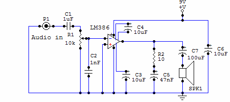
Here is a simple audio amplifier circuit that is easy to build and has few components. This circuit is built around the LM386 audio amplifier integrated circuit, useful when you need to power medium-sized speakers from a music player...
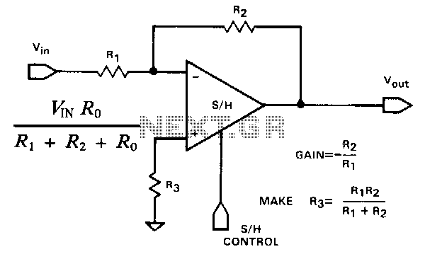
This illustrates another application in which the hookup versatility of a sample-and-hold often eliminates the need for a separate operational amplifier and a sample-and-hold module. This hookup will have a somewhat higher input-to-output feedthrough during hold than the non-inverting...
The non-inverting amplifier has a gain of R2/R3 (1 in this case) and produces a voltage of V during a positive excursion of Vin with respect to ground. The inverting amplifier accommodates the negative excursions of V; its gain...
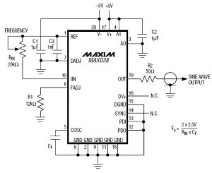
A high-frequency waveform generator is highly beneficial for electronic experimentation and design. This circuit generates sine wave oscillations; however, it can be modified to produce triangle or square wave functions. The frequency can be controlled using current. By disconnecting...
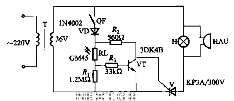
High-voltage isolation switches must not be connected to loads that could create an arc, which may lead to a short circuit between the high-voltage bus and result in accidents that endanger both equipment and personnel safety. Consequently, high-voltage switchgear...
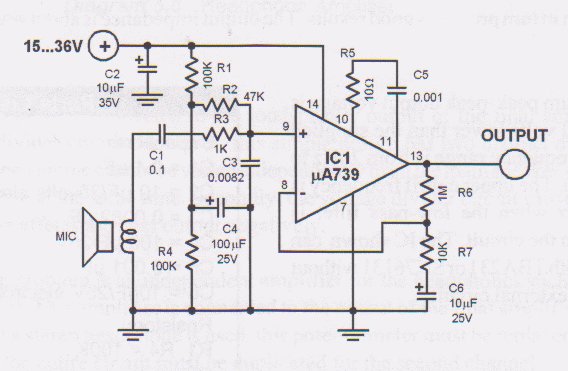
This circuit is a low voltage microphone preamplifier that operates with a 1.5V power supply. It features a reference with a 500 kHz unity-gain bandwidth, functioning as a preamplifier with a gain of 100. The output from this stage...