
Offset-Adjusting Current Source Circuit
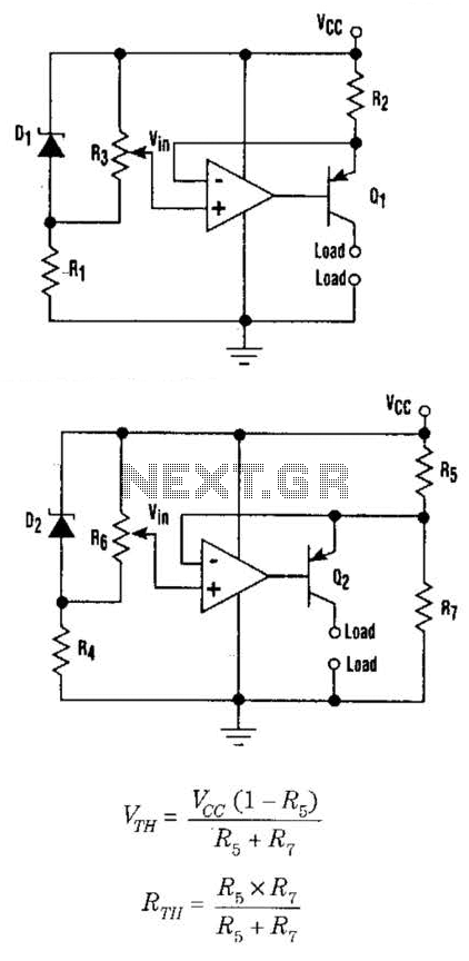
This circuit design emphasizes the importance of managing offset voltages in operational amplifiers to prevent unintended activation of the current source. The primary components involved include the operational amplifier, resistors R2, R7, and others, which are strategically chosen to ensure the desired output characteristics. The inclusion of R7 is critical, as it allows the circuit to maintain functionality across various op-amp specifications by providing a means to counteract the offset voltage that can lead to erroneous current output.
The output current, represented as 70UT, is derived from the relationship between the voltage at the wiper of R3 and the value of R2. This relationship is essential for maintaining the accuracy of the current source, particularly in applications where precise current control is necessary. The circuit's design must account for the maximum offset voltage (Vos) of the op-amp, ensuring that the turn-off condition is met under all specified operating conditions.
Furthermore, the introduction of the Thevenin equivalent voltage and resistance through R7 aids in stabilizing the circuit's performance. By setting Vcc appropriately in relation to R7, it is possible to ensure that the current source remains off when it is not intended to be active. This careful balancing of voltages and resistances is crucial in achieving a reliable and accurate current source.
Overall, the described circuit provides a robust solution for creating a cost-effective current source with a high degree of accuracy, while also addressing the challenges posed by operational amplifier offset voltages. The design principles outlined here can be applied to various electronic applications where precise current sourcing is required, making it a valuable addition to the toolkit of electronic circuit designers. Though this setup can act as a cost-effective current source with an output accurate to 1%, the voltage offset will turn on the current source even when Vqq equals Vin. 2. Modifying the configuration of Figure 1 can rectify the problem of the current source being turned on by the voltage offset.
The addition of R7 allows an adjustment that guarantees turn-off for any op-amp offset specification. By carefully choosing components, you can create a cost effective circuit for a current source with an output that`s accurate to 1% (Fig.
A). 70UT (the current flowing from the collector of Ql) is ^cc^`in (^e voltage at the wiper of R3) divided by the value of R2. In some instances, it`s important to be able to turn off the current source (within the limits of Icm for Ql).
Unfortunately, in about half ofthese cases, the offset voltage (l70S) of the op amp will turn the current source on even when Vcc = Vm. That`s because the offset voltage (when the noninverting input needs to be at a higher potential than the inverting input to get an output of 0 V from the op amp) is impressed across R2.
This offset voltage forces Ql to turn on enough to yield a collector current of V()S divided by R2. Diagram offers a fix for this predicament. The addition of R7 presents the emitter of Q2 with a Thevenin equivalent voltage and resistance represented by: The difference between Vcc and VTH is Vcc + R7). If Vcc (#5/fl5 + R7) is set equal to the maximum Vos spec for the op amp in question, the circuit is then guaranteed to turn off.
This circuit has an output current of VTH - VSN divided by RTI}. The compromise of Fig. does present another error term in the circuit. The term (Vm - ISJN) will have to be 2 Vos to guarantee a current output for whole population of the op amp chosen. This error can be made arbitrarily small (but not zero) by increasing the voltage of D2 and Vcc while raising the value of D2 and Vcc while also raising the value of the equivalent resistance Rth.
🔗 External reference
Related Circuits
The circuit diagram illustrates a dual radio remote control switch system. The transmitter section features Q3, which generates a high-frequency carrier signal, while Q1 and Q2 form the oscillator circuit. Pressing switch SW1 results in an oscillation frequency of...
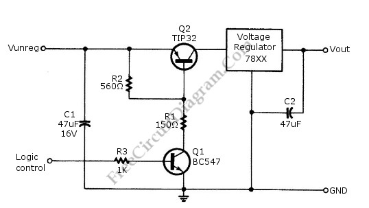
Logic power control of an analog regulator can be useful in applications where a digital circuit or controller needs to manage a power source, such as in EEPROM programmers or other power control systems. This circuit provides ON-OFF control...
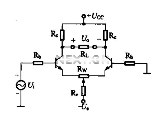
Differential amplifier circuit with four connection methods and characteristics for comparison. The circuit exhibits magnification with a single tube when symmetrical. Additionally, CMRR (Common Mode Rejection Ratio) is adapted from single-ended input to a double-ended output. The differential amplifier is...
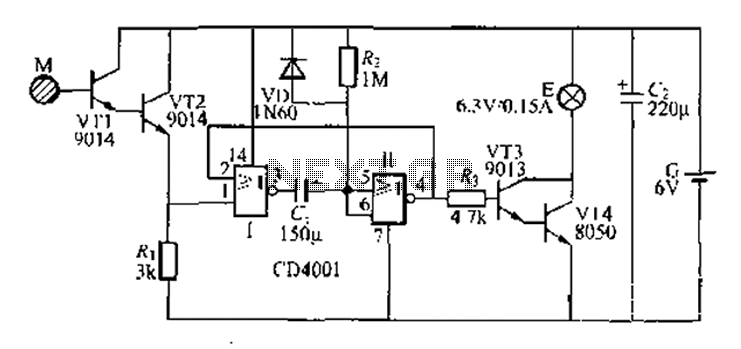
A two-battery powered light touch delay circuit designed for convenience at night. It can be placed on a bed pillow, and when the metal contact M under the capsule is touched, a small lamp will automatically light up. The...

A high-power and efficient 100W power amplifier electronic project can be designed using the STK404 audio power amplifier hybrid ICs. These ICs consist of optimally designed discrete component power amplifier circuits that have been miniaturized using SANYO's unique insulated...
An individual has been studying Nikola Tesla's work for approximately 11 months and recently discovered Imhotep's concept of Radiant energy. The study of Nikola Tesla's contributions to electrical engineering and energy transmission has led to significant advancements in understanding electromagnetic...
Warning: include(partials/cookie-banner.php): Failed to open stream: Permission denied in /var/www/html/nextgr/view-circuit.php on line 713
Warning: include(): Failed opening 'partials/cookie-banner.php' for inclusion (include_path='.:/usr/share/php') in /var/www/html/nextgr/view-circuit.php on line 713