
OP AMP BASED MONOSTABLE MULTIVIBRATOR 741
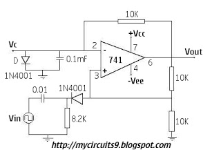
This circuit operates as a monostable multivibrator, which is designed to produce a single output pulse in response to an input trigger. The initial stable state is maintained until a triggering event occurs, which can be a voltage pulse applied to the input. The transition to the quasi-stable state is characterized by the output voltage changing from its stable high state (+Vsat) to a low state (-Vsat) upon receiving a negative trigger.
The function of diode D1 is critical in this configuration, as it clamps the voltage across the capacitor (Vc) to a predetermined level of 0.7V, ensuring that the capacitor does not charge beyond this voltage during the pulse generation process. The feedback voltage of +2Vsat at the non-inverting terminal ensures that the comparator remains in a high state until the triggering condition is met.
When the negative trigger is applied, the potential at the non-inverting terminal drops below the threshold of 0.7V, leading to a rapid switch in the output to -Vsat. This change in output state causes the diode to become more negatively biased than -2Vsat, which effectively turns off the feedback to the non-inverting terminal. As a result, the comparator resets and switches back to +Vsat, initiating the charging cycle of capacitor C.
The charging of capacitor C through resistor R is a crucial part of the timing mechanism of this circuit. The time it takes for the capacitor to charge to 0.7V is determined by the RC time constant, which is a product of the resistance (R) and capacitance (C) values. Once Vc reaches 0.7V, the circuit returns to its stable state, completing the pulse cycle. This design allows for precise control of pulse width and timing, making it suitable for various applications in digital electronics and signal processing.The circuit remains in stable state until a triggering signal is applied to its input. After getting the triggering signal the output transit from stable to Quasi-stable state and return back after a time period. So a Single Pulse isgenerated for single Trigger. Consider the instant at which the output Vo=+Vsat. At that time diode D1 damps the Capacitor voltage, Vc at 0. 7V. Feedback voltage is + ²Vsat at Non-Inverting terminal. When the negative trigger is applied, the potential at Non-Inverting terminal becomes less than 0. 7v the output switches to -Vsat, which makes the diode more negative than - ²Vsat. Comparator switches back to +Vsat. The Capacitor C starts charging to +Vsat through R until Vc reaches 0. 7v and C becomes damped to 0. 7v. 🔗 External reference
Related Circuits
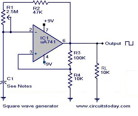
Square wave generator using uA741. Circuit diagram, theory, and working principle. The square wave generator utilizing the uA741 operational amplifier (op-amp) is a fundamental circuit widely employed in various applications, including signal processing, waveform generation, and timing applications. The uA741...
The three stages commonly found in audio amplifiers and operational amplifiers are clearly visible. However, actual audio designs often feature modifications and enhancements in key areas. This overview highlights design improvements in audio amplifiers, focusing on each of the...
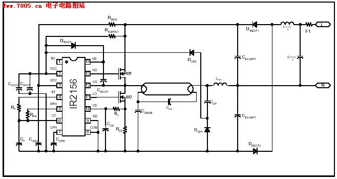
The IR2156 provides a cost-effective solution for fluorescent electronic ballasts. It integrates features such as lighting tube error protection and a programmable working frequency, which includes warm-up, lighting, and continuous operation of the ballast. The IR2156 is a highly integrated...
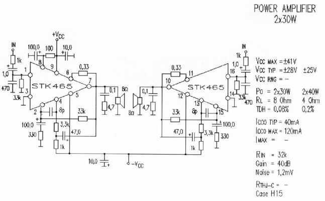
Completed STK465 is an amplifier of acoustic frequencies that offers qualitative output, using minimal exterior elements. Substantially he is one of big completed force. Has a line pins and incorporated metal surface for adaptation in cooler. The provision pins...
The LME49810 audio amplifier schematic is depicted in the accompanying circuit diagram. Based on the LME49810 datasheet, this component is a high-fidelity audio power amplifier driver intended for use in applications such as audio-video receivers, guitar amplifiers, powered studio...
The philosophy behind this minimalist design has been explained by Flavio Dellepiane on his highly interesting site. I have myself written an article about this fleapower amp from Italy in the American magazine AudioXpress. All relevant details are published...
Warning: include(partials/cookie-banner.php): Failed to open stream: Permission denied in /var/www/html/nextgr/view-circuit.php on line 713
Warning: include(): Failed opening 'partials/cookie-banner.php' for inclusion (include_path='.:/usr/share/php') in /var/www/html/nextgr/view-circuit.php on line 713