
Op amp circuit diagram relay delay release
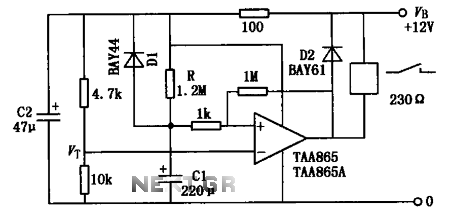
The delayed release operational amplifier relay circuit employs an operational amplifier configured to act as a comparator. The inverting terminal receives a reference voltage through a 4.7k resistor, while the non-inverting terminal is connected to a charging capacitor (C1) that influences the output state of the op-amp. The timing mechanism is governed by the RC time constant formed by the resistor (1.2M) and the capacitor (C1), where the charge time of C1 determines the delay before the relay is activated.
When the circuit is powered, the capacitor C1 starts charging, and the voltage across it increases gradually. The operational amplifier's output remains low until the voltage across C1 exceeds the reference voltage present at the inverting terminal. At this point, the output of the operational amplifier transitions to a high state, activating the relay.
The relay can be utilized for various applications, such as controlling higher power devices or signaling alarms, depending on the load connected. The adjustable resistor (1.2M) allows for customization of the delay, making this circuit suitable for applications requiring precise timing control. The design ensures that the relay remains inactive during the charging phase of the capacitor, thereby preventing premature activation. Overall, this circuit is an effective solution for applications requiring a delay in relay activation. As shown in FIG relay the delayed release operational amplifier circuit. When the power switch, the inverting input terminal of the operational amplifier is added resistor 4.7k and 10k partial pressure of VT, C1 had a chance to charge the non-inverting input is applied low. Therefore, the operational amplifier output is low and relay. And the power to charge the capacitor through resistor 1.2M C1. With the charging capacitor C1, the voltage which is gradually increased over a period of time on the Cl voltage becomes high, so the non-inverting input plus is high, the operational amplifier output is high, the relay It is released. So this circuit is a relay delay release circuit. The length of the delay time can be varied by adjusting the 1.2M resistance, such as by the parameter map, the delay time is about 260s.
Load circuit may be a relay or solenoid coil may be lights and other display and alarm devices.
Related Circuits
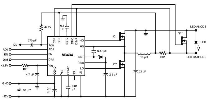
The LM3434 adaptive constant on-time DC/DC buck (step-down) constant current controller can be used to design a simple high-power LED driver application. The LM3434 provides a constant current for illuminating high-power LEDs. The output configuration allows the anodes of...
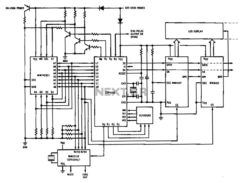
A compilation of dial phone numbers, including 15 commonly used libraries and the dialed number, is stored in standard CMOS RAM. A single-button keypad facilitates the input of a phone number, which can be dialed directly or stored in...
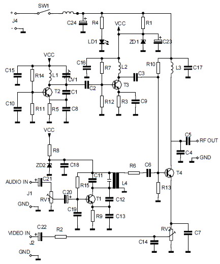
The circuit converts audio and video signals into a UHF TV signal, allowing a video signal from a camera or other source to be connected to a standard TV set. The audio and video signals are transformed into a...
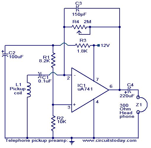
This circuit utilizes the uA741 integrated circuit to capture voice signals from telephone lines without direct contact. By positioning a high-impedance magnetic core near a telephone device or along the telephone wires, the circuit can inductively pick up both...
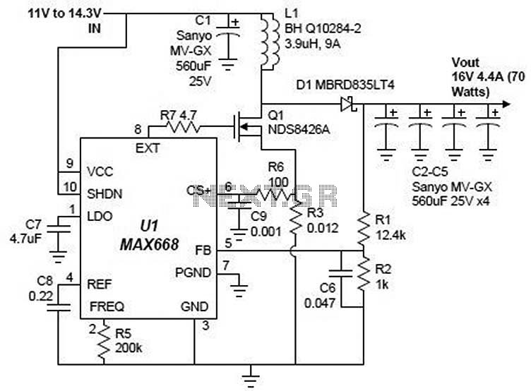
A simple 16-volt switching power supply circuit can be constructed using the provided diagram, which is based on the MAX668 constant-frequency, pulse-width modulating (PWM), current-mode DC-DC controller. This integrated circuit is designed for a wide range of DC-DC conversion...
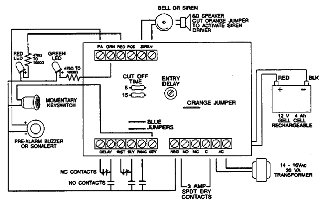
The following alarm circuit is designed with features that may be suitable for residential and commercial alarm system applications. It has a 12V and 1.5A regulated power supply. Furthermore, this residential alarm circuit also includes a delay circuit, a...