
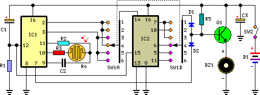
op amp ringer circuit old telephone

The circuit in question involves a ringer circuit designed to operate with a high output voltage, typically required for ringing functionality in telecommunication devices. The initial observation of a 45V output when only a portion of the schematic is connected suggests that the circuit includes a step-up (boost) converter or a charge pump that increases the voltage from the input source. This behavior is indicative of a design intended to generate a high ringing voltage necessary for the phone's operation.
Upon connecting the ringer circuit, the output voltage drops significantly to about 7 volts. This phenomenon can be attributed to several factors. First, the ringer circuit may have a higher load demand, leading to a voltage drop due to insufficient current supply at the lower input voltage. The initial 3.5V supply may not be adequate to maintain the required voltage under load conditions, resulting in the observed drop.
Additionally, the design of the ringer circuit may inherently require a minimum input voltage to function correctly. As noted, increasing Vcc to 9V allows the output voltage to rise to 18V, which is still below the expected 45V but indicates a direct relationship between the input voltage and the output capability of the circuit. The requirement for a higher Vcc suggests that the ringer circuit may be designed to operate optimally at voltages higher than 3.5V, possibly due to internal resistances or component ratings that necessitate a stronger input to produce the desired output.
To address the issue of low output voltage when connecting the ringer, it is advisable to review the circuit design and component specifications. Ensuring that the boost converter or step-up circuit is capable of delivering the necessary voltage under load conditions is crucial. Furthermore, examining the current draw of the ringer circuit and optimizing the power supply to meet this demand will help achieve the desired ringing voltage without requiring excessive input voltage.In the process of adapting an old phone to be used as an Bluetooth phone. I am currently testing the ringer circuit, which I build using the schematics provided by Sparkfun. Now, when I hook up just the right part of the schematic to a 3. 5V source (Vcc), I get a nice 45V on the output (with a steady current draw of about 130mA). But as soon as I connect this to the ringer part, I measure an output voltage of only about 7 volts. Increasing Vcc keeps the `45V`-voltage at about twice the Vcc. I have to turn up Vcc to about 9V to get the `45V`-voltage to about 18V, and then phone rings if I set RING1 and RING2 alternately to high (alternating at roughly 20Hz). It is not very loud, but it does work. My question: why do I measure a lower voltage at the 45V output when I connect the ringer circuit Why does this drop to a lot lower values I don`t want to need to provide 10V to the schematic, for what I know it should run on 3.
5V. 🔗 External reference
Related Circuits
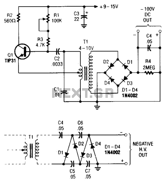
The combination of a Hartley oscillator and a step-up transformer can generate significant negative high voltage, particularly when the voltage output of the transformer is multiplied by the circuit. The Hartley oscillator is a type of LC oscillator that utilizes...
This circuit is designed to drive an ultrasonic transducer. A question has arisen regarding how to limit the output current, as a 60W transducer may be at risk of damage due to excessive current. Guidance or examples for integrating...
The circuit involves a Signetic balance modem connection utilizing a transistor array as a phase detector. It provides information about the cosine of the phase angle, which corresponds to the frequency of the input signal combined with the integrated...
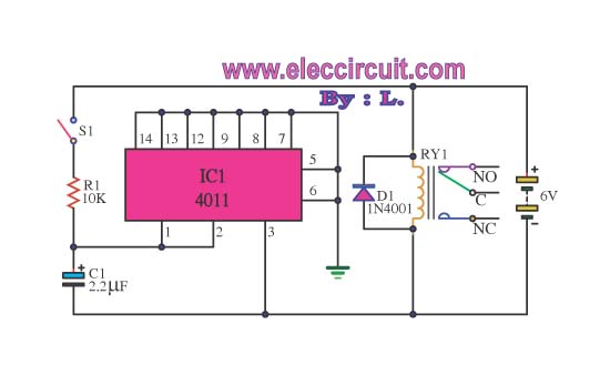
This circuit illustrates the use of the 4011 integrated circuit (IC) for a surge protection electronic circuit diagram. Features include the ability to delay the activation of other appliances connected to the output. The 4011 IC is a quad 2-input...
This timer is designed for individuals seeking to achieve a tan while minimizing excessive exposure to sunlight. A rotary switch allows the user to set the timer based on six classified photo-types. A photoresistor adjusts the preset time value...
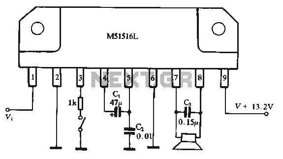
Figure 1-44 illustrates a dedicated BTL (Bridge-Tied Load) amplifier circuit, which consists of two single amplifiers. The relevant components are integrated into the circuit, simplifying the connections. The circuit operates at a power supply voltage of 13.2V and can...