
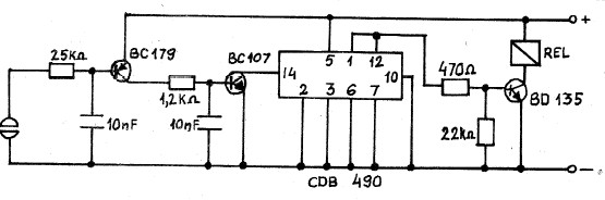
op amp Why do some of my IE converter circuits have a large offset voltage

The circuit employs a feedback mechanism to stabilize the inverting input, ensuring accurate current measurements in the nanoamp range. The use of a 10K resistor allows for a defined low state when the circuit is idle, preventing noise and ensuring stability. The ADG1236 CMOS switch facilitates precise control over the feedback resistor selection, which is crucial for setting the gain of the current measurement circuit. Given the sensitivity of the application, the low leakage currents of the switches are paramount; however, variations in performance across different production batches have led to inconsistencies in offset behavior.
The phenomenon of slow-decaying offsets on certain boards may be attributed to several factors, including potential variations in the manufacturing process, differences in component tolerances, or PCB layout issues that could introduce additional parasitic capacitances or resistances. The calibration process, which relies on measuring the output with an open input, is an effective method for mitigating constant offsets; however, the persistent accumulation of offsets upon power cycling suggests that the underlying issue may not be solely related to the operational characteristics of the switches.
Further investigation into the affected boards may involve detailed analysis of the PCB layout, examination of the power supply stability, and testing of individual components to identify any anomalies. Additionally, implementing a more robust calibration routine or exploring alternative switch technologies with even lower leakage currents may help to enhance the stability and reliability of the circuit across all production batches.The inverting input is held low through a 10K resistor when the circuit is powered on but not being used. Whenever a measurement is being made (including calibration measurements where IN is floating), that resistor is disconnected.
The circuit is used to measure currents in the nanoamp range. A few mV on the output is significant. Constant offsets are not really a problem, as they can easily be calibrated out by measuring the output with an open input and subtracting that from subsequent measurements. SW1A and SW1B are different poles of the same CMOS switch (ADG1236). They are switched together to select the feedback resistor, which determines the gain of the converter.
The maximum leakage current is 1 nA on source and drain pins, on or off. The switch not shown (for holding the inverting input low through a 10K resistor) has similar performance. Typical leakage currents are very small (< 0. 1nA). The problem I am having is that in some batches of boards, some (or all) of these circuits have large offsets which decay slowly when powered on.
However, most boards are perfectly stable at all times, with small offsets. When the afflicted boards are powered on, the offset will slowly (after hours of days) stabilize to ~5 mV. After power is removed, the offset accumulates again, so when powering it on after a couple days of being off, it`s high again.
Each board has a bunch of these circuits on it. In the first batch of 5 boards, all of them were affected. In the next batch, none were affected. In the most recent batch, each board has one affected circuits, and it isn`t always the same one. At the worst case, the maximum leakage currents of all the analog switches would be 1. 2nA, resulting in a 12 mV offset at the highest gain setting, so I don`t think that can account for all the offset I`m seeing. 🔗 External reference
Related Circuits
The TPS3803 and TPS3805 families of supervisory circuits offer circuit initialization and timing supervision, mainly for digital signal processors (DSPs) and processor-based systems. The TPS3803G15 device features a fixed-sense threshold voltage (VIT) determined by an internal voltage divider, while...
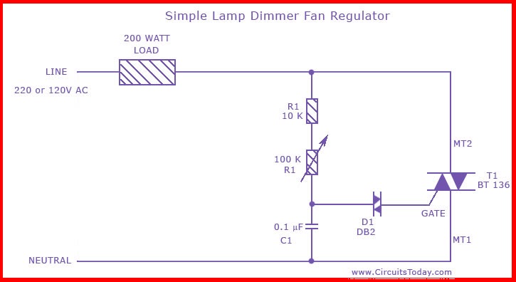
This is the circuit diagram of the simplest lamp dimmer or fan regulator. The circuit is based on the principle of power control using a Triac. The circuit operates by varying the firing angle of the Triac, which is...
TIP141 is an NPN silicon power Darlington transistor designed for complementary use with TIP145, TIP146, and TIP147. It can handle up to 125 W at a case temperature of 25 °C, with a continuous collector current of 10 A...
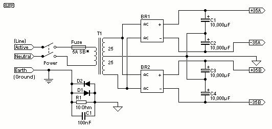
For the 60W amplifier, a nominal (full load) supply of +/- 35V is required, so a 25-0-25 secondary is ideal - however, see Updates, below. The circuit for the supply is shown below, and uses separate rectifiers, capacitors and...
A collection of touch switch circuits is presented. A touch switch is an electronic device that allows control of a circuit simply by touching a sensor. The circuit diagram illustrates a simple design that utilizes only eight components. The...
The color of the LED makes a significant difference. The type and size of the LED, such as 3mm or 5mm, and the power source are crucial factors to consider. More information is required for accurate calculations. A basic...
Warning: include(partials/cookie-banner.php): Failed to open stream: Permission denied in /var/www/html/nextgr/view-circuit.php on line 713
Warning: include(): Failed opening 'partials/cookie-banner.php' for inclusion (include_path='.:/usr/share/php') in /var/www/html/nextgr/view-circuit.php on line 713