
op amp Why does this current limiter circuit oscillate

The circuit described is a current limiter designed to regulate the output current through a resistive load based on a control voltage. The primary components include two operational amplifiers, O1 and O2, which are configured to form a feedback loop to maintain the desired current output. The O2 op-amp is set up as a differential amplifier with a gain of 2, allowing it to amplify the voltage across the load (R2) to the required level for the feedback loop.
In operation, when a control voltage of 0-5 V is applied, the goal is to produce a corresponding output current ranging from 0 to 25 mA through the load. The output from the O2 op-amp, marked as CSense, is expected to be 5 V when the load is at maximum current. However, oscillation issues have been reported, indicating that the feedback loop may not be stable under certain conditions.
The oscillation behavior observed, with frequencies varying from 50 kHz to 150 kHz, suggests that the system may be experiencing instability due to the non-linear characteristics of the MOSFET used in the circuit. As the control voltage increases, the amplitude and frequency of the CSense signal also change, indicating a potential mismatch in the expected and actual behavior of the feedback loop.
To address these oscillation issues, it is recommended to introduce a damping mechanism by adding resistance in series with the input signal to the negative input of O1, along with capacitance between the output of O1 and its negative input. This modification can help stabilize the circuit by reducing the gain at certain operating points, thus preventing oscillations.
Additionally, it is advised to consider replacing the MOSFET with a PNP transistor in the circuit design. Given that the required compliance range is only 5 V (200 ohms multiplied by 25 mA), using a PNP transistor with an appropriate emitter resistor can provide a more linear current source while simplifying the design. The transistor can be configured with its collector connected to the controlled current output and its base driven directly by the output of the op-amp, ensuring that the output can swing sufficiently close to the positive supply voltage.
Overall, careful attention to the feedback loop design and component selection will be crucial in achieving a stable and reliable current limiting circuit.Make a 0-25 mA current limiter. I want to take a control voltage of 0-5 V as input and have it control a current of 0-25 mA through a restive load (the restive load may vary between 0-200, it`s represented as R2 below). The O2 op-amp is used to make a differential amplifier with a gain of 2. Example: 25mA of current through the lo ad R2, op-amp O2`s output should be 5V (marked CSense). The output from op-amp O2 is then the input to op-amp O1. Op-amp O1 compares the control voltage with O2`s feedback to limit the current. Or at least that`s my intention. I have triple checked my pin-out and wiring, and messed around with lots of other things, but the circuit still just oscillates. When V2 is a higher value the oscillation is slower. What I am seeing on the DSO is that mosfet T1 goes between full on and full off, and CSense is a triangle wave that varies in amplitude with the control voltage.
A higher control voltage makes CSense have higher amplitude and lower frequency. The oscillation frequency varies from about 50kHz to 150kHz. Update Everyone is focusing on O1, but I think the problem is in the O2 circuit. Below is a DSO screen shot. V2 is at 1. 25 VDC. The yellow trace is the voltage over R2 @ 100. The red trace is the output of O2 (marked as CSense in my schematics). I would expect the red trace to be 2x the yellow trace, but instead it`s a completely different shape! What in the world is going on For clarity: I would expect the yellow line to be 0. 625 VDC, and the red line to be 1. 25 VDC (same as the V2 input). Also my power supply is ~8 VDC here, things blow up at 24. The V2 input is a sine wave. The output is supposed to follow the input. If you change V2 to DC, the output will also simulate as DC. On my bench, V2 is DC, but the output oscillates between 30kHz-250kHz. Imbue Apr 12 `13 at 15:38 Is the second op-amp slewing According to the datasheet, the slew rate is 0.
5V/us. If I read your o-scope capture correctly, the rise and fall time for the red trace is approximately the slew rate of the OPA2170 Alfred Centauri Apr 12 `13 at 17:03 Also note how R2 introduces a common mode swing to the inputs of OA2. Crappy old parts like TL0XX do not have good rejection for that (as low as 75 dB). Why introduce it Kaz Apr 12 `13 at 17:17 The problem is that the current thru M1 as a function of gate voltage is highly non-linear.
At some point in the function, the gain is very high, which is making things unstable. If you don`t need high speed response from this circuit, you can dampen it somewhat past the point where you experimentally determine it won`t oscillate at any operating point. To do that, add some resistance in series with the input signal going into the negative input of O1, then add some capacitance immediately between the O1 output and its negative input.
Due to the non-linear nature of the current source this is driving, the capacitance value that guarantees no oscillation over any part of the operating range will also overdamp the system at others. That may be OK if you`re not looking for fast response. I would do the above anyway, but I wouldn`t use a FET in the first place. You only need a 5 V compliance range (200 © times 25 mA), so you have plenty of voltage headroom. You have 24 V to start with. The load can take up to 5 V, and the current sense resistor another 2. 5 V. That leaves 16. 5 V headroom for the current source. You really don`t need all that, but you can easily spend 5 V or so to get a reasonably linear current source.
Ditch the PFET and use a PNP transistor with 200 © or so in series with its emitter. The other end of the resistor is tied to the 24 V supply, the collector becomes the controlled current output, and the base is driven directly by the opamp output. This assumes the opamp output can swing to within half a volt of the positive supply, which many can`t.
The top schematic doesn`t specify the opamp at all, and 🔗 External reference
Related Circuits
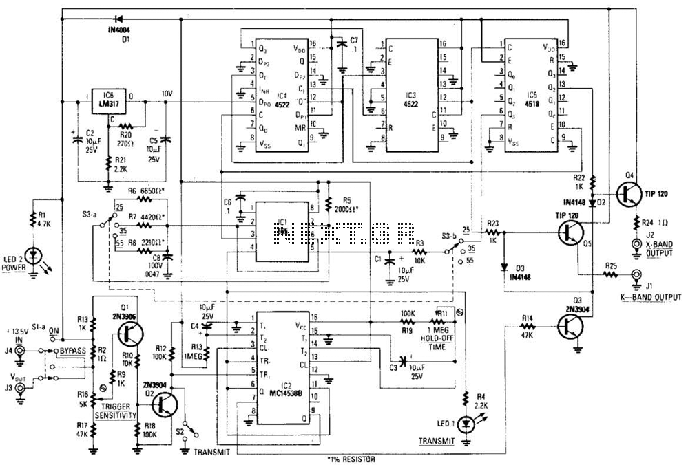
This circuit is a system designed to generate a pulsed modulation signal for a Gunn diode microwave oscillator. It features several preset speed settings (S3 a and b). A 555 timer is employed in conjunction with a frequency divider...
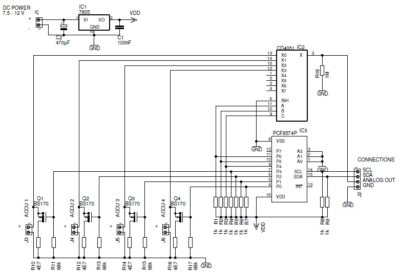
This page describes a battery tester designed to characterize batteries and save the results on a microSD card. The battery tester circuit is engineered to evaluate the performance and capacity of various battery types, providing accurate and reliable data storage...
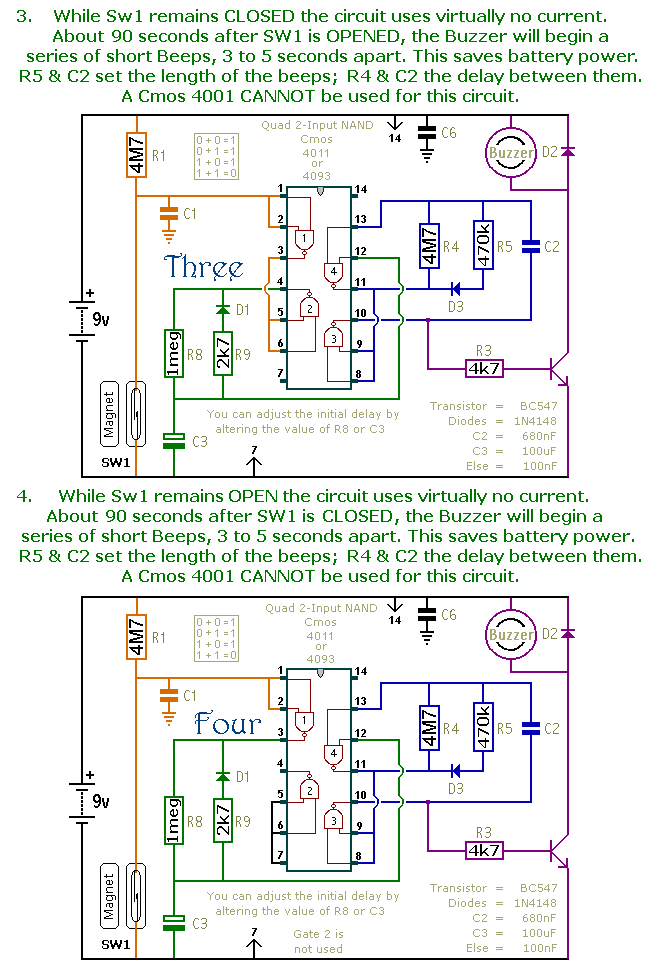
This document presents a collection of compact, self-contained alarm circuits. These circuits are designed to operate with a very low standby current, making them ideal for battery-powered applications. They can be triggered by both normally-open and normally-closed switches, while...
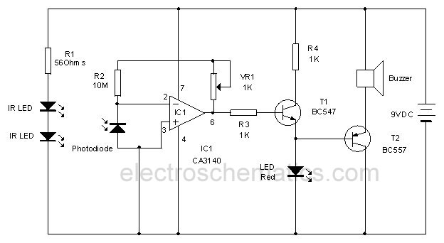
This infrared alarm barrier is designed to detect individuals passing through doorways, corridors, and small gates. The transmitter emits an infrared light beam that is not visible to the human eye. When the beam is interrupted by a person,...
The MK484 AM receiver circuit is a simple design based on the MK484 AM receiver IC from Rapid Electronics Ltd. The MK484 is a monolithic integrated circuit that incorporates all necessary sections of an AM receiver, including an RF...
There are numerous circuits designed for low voltage regulators. However, for higher voltages, such as those required for valve circuits, the approach differs. This is the reason for the design of a simple regulator capable of handling these voltages....