
Opamp Based Power Amplifier
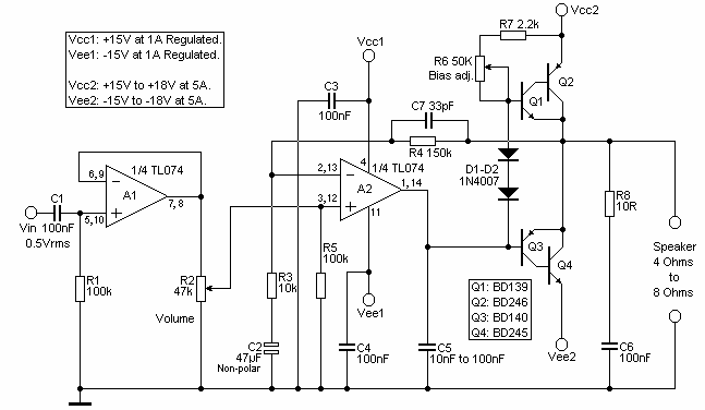
The class-AB amplifier configuration is a widely adopted design due to its efficiency and linearity, which makes it suitable for audio applications. It operates by using two or more output devices that function in complement to each other. The compound pair output transistors, also known as Sziklai pairs, offer benefits such as improved linearity and higher input impedance, which are critical for achieving the desired audio quality.
The TL074 quad opamp, a Low-Noise JFET-Input Operational Amplifier, plays a crucial role in this system. It is responsible for driving the output transistors, which in turn helps to amplify the input signal. This opamp is characterized by its high slew rate and low input bias and offset currents, making it a suitable choice for high fidelity and audio applications.
The voltage gain of the amplifier is determined by the opamp A2. The equation for the overall voltage gain of the amplifier is (R4 / R3) + 1, which is the standard gain equation for a non-inverting operational amplifier. In this particular case, the gain is either 16 or 24dB, which is a substantial amplification factor.
The schematic also implies that the voltage gain of a common collector stage is assumed to be unity. This is a reasonable assumption as a common collector, or emitter follower, is typically used for impedance matching and does not provide voltage gain. The unity gain of the common collector stage, therefore, does not contribute to the overall amplification of the circuit.
In conclusion, this amplifier circuit combines the efficiency of a class-AB amplifier, the high input impedance of the compound pair output transistors, and the high slew rate of the TL074 quad opamp to achieve a substantial voltage gain of either 16 or 24dB.The amplifier is based on the commonly used class-AB complementary power amplifier with compound pair output transistors. The system uses a TL074 quad opamp to drive the output transistors. As can be seen from figure 1, A2 is used to set the voltage gain of the amplifier. Assuming the voltage gain of a common collector stage to be unity, the overall voltage gain of the amplifier is equal to (R4 / R3) + 1, i.e.
the gain of a non-inverting OP-AMP (16 or 24dB, in this case). 🔗 External reference
Related Circuits
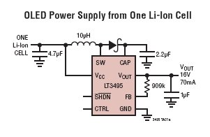
The LT3495, LT3495B, LT3495-1, and LT3495B-1 are low-noise boost converters equipped with an integrated power switch, feedback resistor, and output disconnect circuitry. These devices manage power delivery by adjusting both the peak inductor current and the switch off-time, resulting...
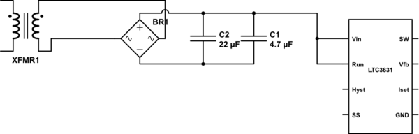
The leads from the transformer to the circuit are quite long (>5m). The 110V side of the transformer has been switched off frequently, which likely caused a spike on the secondary (24V) side. The input pin of the LTC3631...
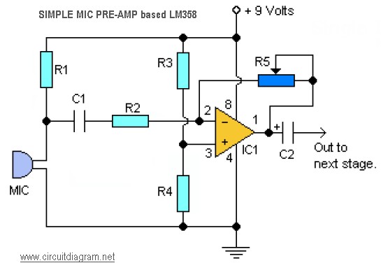
This is a simple audio microphone preamplifier circuit based on a single LM358 IC. The circuit is straightforward, cost-effective, and easy to construct. The component parts list includes: R1, R3, R4 = 10K; R2 = 1K; R5 = 100K-1M...
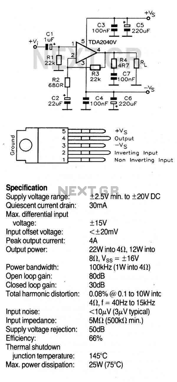
This circuit utilizes the TDA2040V, a monolithic power amplifier integrated circuit designed for high-quality, class AB audio amplification. It typically delivers 22W of output power into a 4-ohm load with a distortion level of 0.5%, powered by a 32V...
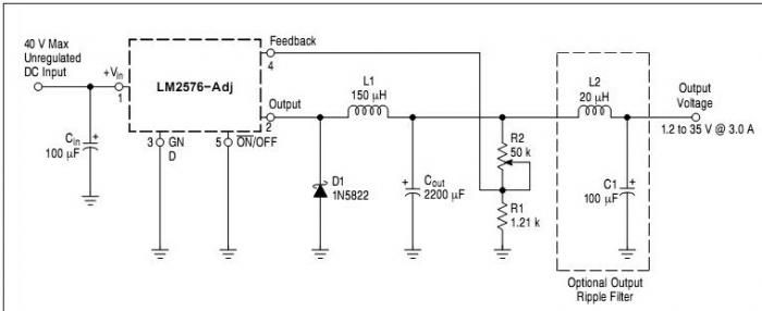
A simple lab power supply electronic project can be designed using this circuit diagram, which is based on the LM2576 monolithic integrated regulator that provides all the active functions for a step-down (buck) switching regulator. As seen in the...
This circuit performs a rapid battery test without requiring a power supply or costly moving-coil voltmeters. It features two ranges: when SW1 is configured as depicted in the circuit diagram, the device can test batteries ranging from 3V to...