
Open source USB scope

The proposed electronic schematic outlines a high-speed data acquisition system designed for a sampling rate of 100 Msps, with future scalability to 1 Gsps utilizing interleaved ADCs. The system begins with BNC probe inputs that connect to a 1 MΩ resistor in parallel with a 20 pF capacitor, enabling input signal compensation. The buffered signal is processed through a high-speed JFET operational amplifier (OPA656), which provides a stable gain without introducing significant distortion or noise. The buffered output then enters a summer circuit, which integrates a bipolar offset generated by a digital-to-analog converter (DAC) to adjust the signal level appropriately before amplification.
The programmable gain amplifier (PGA) follows, allowing for dynamic adjustments to the signal amplitude based on the input range requirements, which are specified to be between 500 mVpp and 5 Vpp. This flexibility is critical for various applications, including software-defined radio (SDR) implementations. The output from the PGA is then sent to an analog-to-digital converter (ADC) for digitization.
A key design consideration is the input overload protection mechanism, which utilizes diodes to safeguard against overvoltage conditions. However, this design is prone to failure, necessitating careful consideration of input signal levels to prevent damage to the circuit.
Future modifications may simplify the design by eliminating the DAC and PGA if the system operates effectively with AC-coupled signals. The architecture could be optimized to include a direct ADC interfaced with an FPGA, which would manage data acquisition and communication with a host computer via a suitable interface, potentially a PCIe bus to accommodate higher data transfer rates.
This schematic design aims to provide a robust, high-speed digitizing solution suitable for continuous data capture, addressing the needs of modern applications while maintaining flexibility for future enhancements.There are plans to make it 1Gsps in the future, using interleaved ADCs and staggered clock, but that`s beyond me at the moment, so the first iteration will only have 100Msps (fastest from single ADC). The part I`m most unsure about is the analog front end, as we haven`t done any high speed circuit design in classes yet, so most of my knowledge com
es from random places on the internet. Would be great if anyone wants to take a look Input from BNC probes go into a 1Mohm resistor in parallel with 20pF (so the probes can compensate for it). The signal is buffered by a wideband, unity-gain stable JFET op amp (OPA656), before being fed to a summer (the pre-amp of the programmable gain amplifier), that adds a bipolar offset from a DAC to the signal.
Then it goes to a programmable gain amplifier, and finally the ADCs. The problem with that front end is that there is that the input overload protection will blow very easily. Any overvoltage input is directly shorted by the diodes - bad news! Perhaps, with modifications, it could be used as a digitizer card for SDR (software defined radio, GNUradio in particular) 100Msps is very fast for a continuous capture digitizer card.
The analog requirements are much simpler - 50 ohm or 75 ohm input, perhaps only a 500mVpp to 5Vpp or so input amplitude range, and much less need for overload protection. In power electronics, transistors should ideally be either fully on or fully off, because a half-on transistor just makes a really poor imitation of Tiffany Yep.
The problem with that front end is that there is that the input overload protection will blow very easily. Any overvoltage input is directly shorted by the diodes - bad news! I`m doing internship right now (as a software developer), so this is my evening and weekends project.
Hopefully I can finish (or at least finish most of) it before school starts again in 8 months. Perhaps, with modifications, it could be used as a digitizer card for SDR (software defined radio, GNUradio in particular) 100Msps is very fast for a continuous capture digitizer card. The analog requirements are much simpler - 50 ohm or 75 ohm input, perhaps only a 500mVpp to 5Vpp or so input amplitude range, and much less need for overload protection.
I`m not sure what you meant by continuous capture. Does that mean streaming samples That won`t work unless we make it a PCI[-E] card or something, since USB 2. 0 would limit the rate to about 40Msps, 1 channel. Also, if the smallest signal is 500mVpp, AC coupled (sounds like it to me), a lot of the circuitry can be taken out - the DAC for offset, and programmable gain amplifier.
I suppose it can just be an ADC with an FPGA coordinating the acquisition, and whatever interface chip to connect it to the computer. I`m not sure what you meant by continuous capture. Does that mean streaming samples That won`t work unless we make it a PCI[-E] card or something, since USB 2.
0 would limit the rate to about 40Msps, 1 channel. Also, if the smallest signal is 500mVpp, AC coupled (sounds like it to me), a lot of the circuitry can be taken out - the DAC for offset, and programmable gain amplifier. I suppose it can just be an ADC with an FPGA coordinating the acquisition, and whatever interface chip to connect it to the computer.
Continuous capture means the ADC is constantly sampling at the rate you desire and send every sample to the host system. Unlike an oscilloscope that only sends parts of acquisitions to the host system. My old Dell HDTV card (~9 years old, came in a used Dell GX110) has only an 8 bit ADC. It worked nicely back in the days, but can`t even come close to the modern cards that use 10 bits or more.
What`s interesting about it is that the decoder chip (Micron) appears to be a general purpose DSP or FPGA since there`s 8MB of DRAM and 512k of Flash on the board. (Too bad there`s no datasheet available, or I`ll reprogram it to operate as a digitizer card, complete
🔗 External reference
Related Circuits
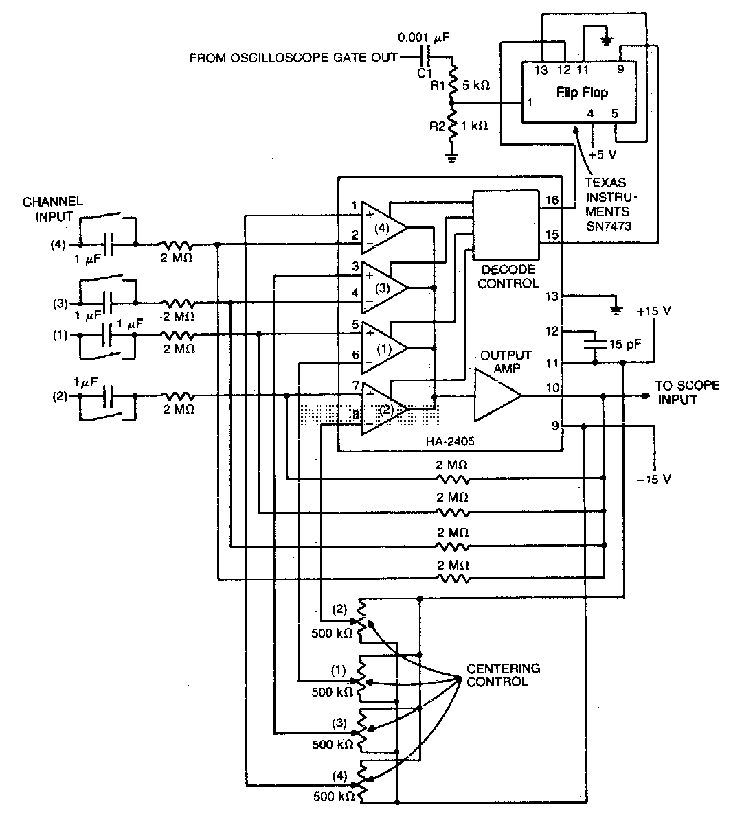
The monolithic quad operational amplifier offers a cost-effective solution for enhancing the display capabilities of a standard oscilloscope. Binary inputs control the integrated circuit operational amplifier, while a dual flip-flop divides the oscilloscope's gate output to generate channel selection...
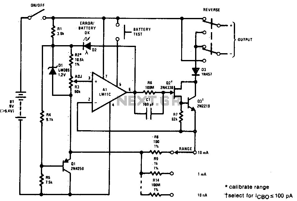
This precision current source features output current ranges from 10 µA to 10 mA, with an output compliance of 30 V to -5 V. The output current is fully adjustable within each range using a calibrated ten-turn potentiometer. An...
The second program sends "Hello world" to the PC. By default, the board utilizes the Virtual COM Port (VCP) driver, allowing output to be viewed using Hyperterminal or similar software; PuTTY is recommended. The setup is straightforward: upon connecting...
The F232 device is powered via USB, but it requires a level translator at its output. The transmit (Tx) signal from the F232 must be converted to RS232 levels, as the receiving side has a maximum voltage requirement. The...
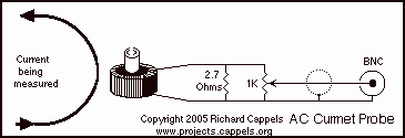
The probe described here was designed to be used over the range of several tens of Hz to a couple MHz with currents from a few tens of milliamps to about 10 amps peak-to-peak. Formulae are given which will...
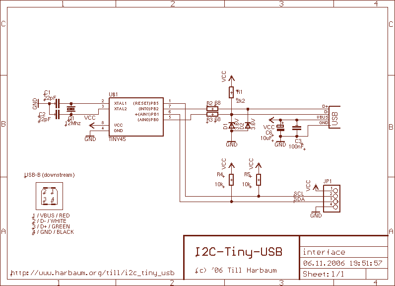
The i2c-tiny-usb project is an open source/open hardware project. The goal of i2c-tiny-usb is to provide a cheap generic i2c interface to be attached to the usb. It is meant as a replacement for those simple and cheap printer...