
Original 2N2/40 Schematic Diagrams

The described receiver section is integral to the overall functionality of the transceiver, facilitating the reception of radio frequency signals and their subsequent processing. The post-mixer amplifier enhances the signal strength after mixing, which is crucial for maintaining signal integrity. The variable crystal filter allows for selective frequency filtering, ensuring that only desired signals pass through while rejecting unwanted noise. The intermediate frequency (IF) amplifier further amplifies the filtered signal, enhancing sensitivity and dynamic range.
The product detector serves as the demodulation stage, converting the IF signal into audio or baseband signals suitable for further processing. The local oscillator generates a stable frequency reference essential for mixing, allowing the transceiver to operate effectively across different frequency bands. Receiver muting is implemented to reduce noise during transmission, preventing interference during switch-over periods.
In the transmit section, the local oscillator again plays a pivotal role, providing the necessary frequency for the transmit single balanced mixer. The transmit RF amplifier boosts the power of the signal for effective transmission, while the driver stage prepares the signal for the final amplifier. The final amplifier, utilizing three parallel-connected 2N2222A transistors, is designed to deliver high output power while requiring robust heat sinks to manage thermal dissipation.
The output low-pass filter is essential for suppressing harmonics and ensuring that the transmitted signal complies with regulatory standards. The Rx/Tx driver facilitates seamless switching between receive and transmit modes, while the receive T/R switch directs signals appropriately based on the mode of operation. The power input circuitry ensures stable voltage and current supply to the transceiver, and the gain switch for the receive RF amplifier allows for adjustable sensitivity based on varying signal conditions, optimizing performance across different scenarios.
Overall, this transceiver design incorporates a well-thought-out architecture, ensuring reliable operation and high performance in both receive and transmit modes.This is the remainder of the receiver, including the post mixer amplifier, variable crystal filter, i. f. amplifier, product detector, local oscillator, receiver muting, and audio amplifier. The transmit section, showing the local oscillator, Tx single balanced mixer, transmit r. f. amplifier, driver, final amplifier, and output lowpass filter. The f inal uses 3 parallel connected 2N2222As in metal cans. Good heatsinks are required. Additional small, but important, pieces of the transceiver design, which include the Rx/Tx driver, the receive T/R switch, power input circuitry, and the receive r. f. amplifier gain switch. 🔗 External reference
Related Circuits

The circuit produces a pleasing and accurate imitation of sound, making it suitable for sound effects such as doorbells. It generates a two-tone effect that closely resembles the sound of a cuckoo. This circuit is designed to create a two-tone...
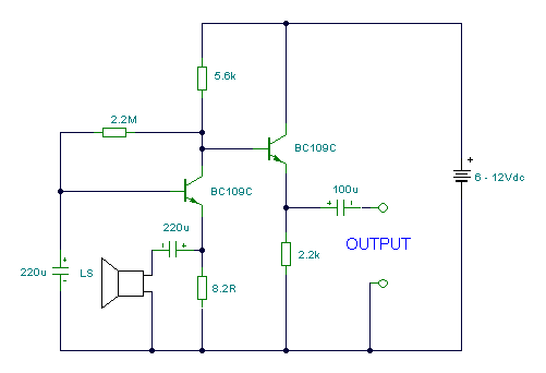
This circuit allows the use of an inexpensive loudspeaker as a microphone. Sound waves that reach the speaker cone cause fluctuations in the voice coil. The movement of the voice coil within the speaker's magnetic field generates a small...
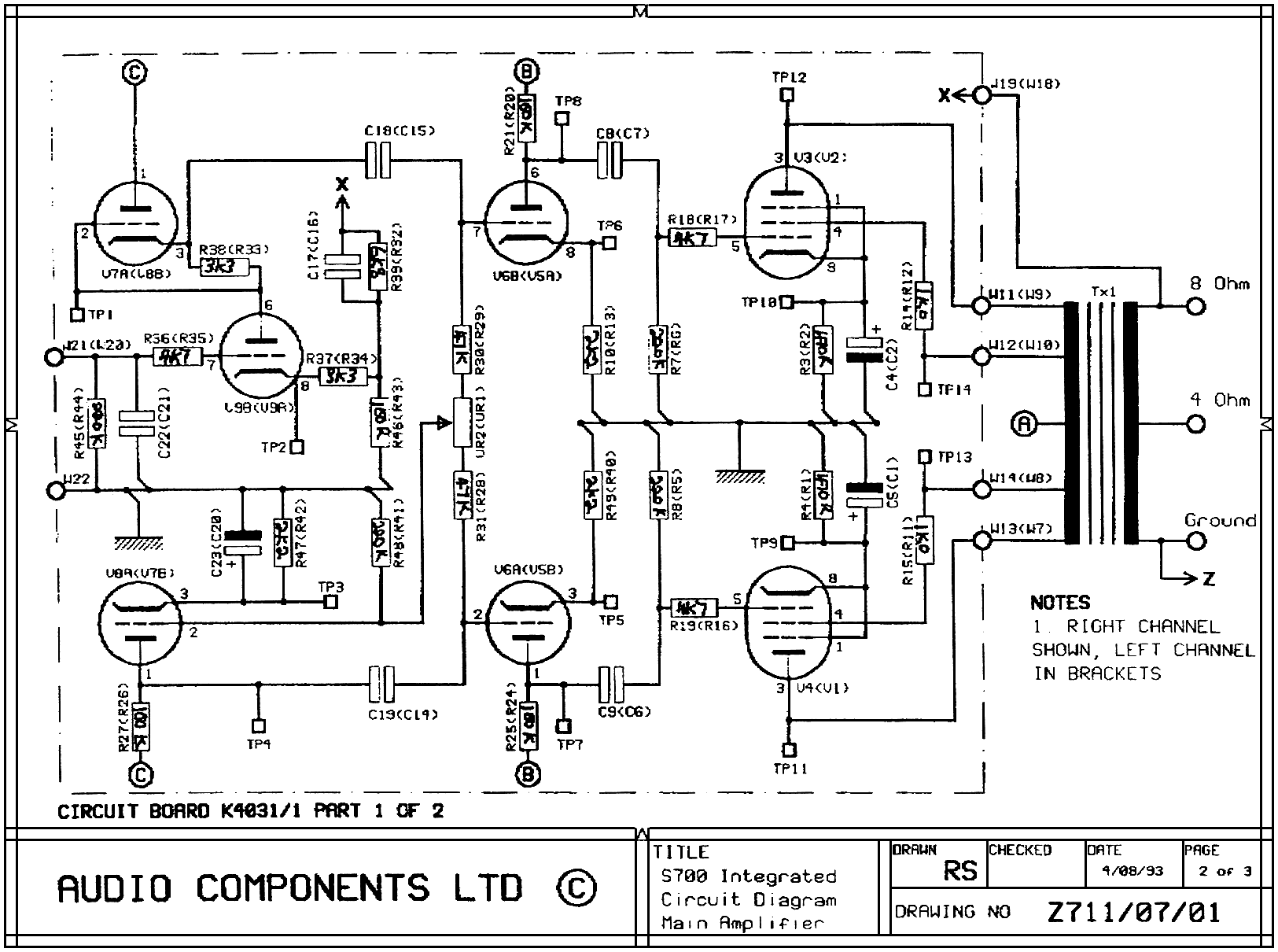
Excessive complexity can lead to confusion. The initial goal was to design a straightforward 15W triode and 30W Class AB1 pentode push-pull amplifier. Class AB1 is chosen because... The design of a 15W triode and 30W Class AB1 pentode push-pull...
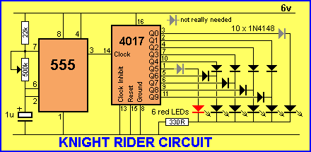
Some simple 555 and flip-flop circuits are being developed to add electronic lighting effects to modernize games. Various circuits are being collected for different game aspects, such as idle states, flipper shots, flower openings, winning shots, etc. A collection...
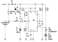
The sections available in this datasheet cover general design considerations for the 555 timer, frequently asked application questions (FAQ), design formulas, and examples of innovative applications. Examples of applications include a Missing Pulse Detector, Pulse Width Modulation (PWM), Tone...
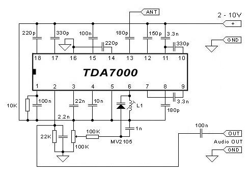
The FM radio receiver circuit is designed using the TDA7000 integrated circuit (IC). This circuit operates with a DC voltage range of 2 volts to 12 volts. The TDA7000 IC is specifically engineered for FM reception and employs a...