
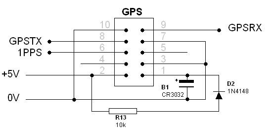
Oscillator Control & GPS
This circuit design effectively addresses the need for precision and stability in generating control voltages for reference oscillators. The use of two parallel 6-bit PWM converters enhances the performance of the system by allowing for higher ripple frequencies, which are easier to filter out. The careful selection of resistors and capacitors ensures that the output voltage is both linear and stable, minimizing the impact of noise. The provision for buffer amplifiers and adjustments for different oscillator types further enhances the versatility and applicability of the VNGBOX microcontroller in various electronic applications.The VNGBOX micro needs to produce a very accurate, high resolution and very noise-free DC control voltage to steer the reference oscillator phase accurately. Any noise on this signal will result in noise on the reference; any non-linearity, especially any unexpected steps in the digital to analog conversion, will result in stability problems.
The circuit is able to generate a very accurate and linear 12-bit DC voltage from 0V to 5V (4096 steps of about 1mV). The micro operates two parallel 6-bit PWM converters, which operate synchronously. Each converter uses six bits of the 12-bit control word. The most significant bits are output on signal EFC6, and the least significant on EFC0. Since the most significant bits have 64 times the significance of the least significant bits, the two signals need to be combined with this gain ratio.
A PWM D-A converter usually operates with a low-pass filter, and this design is no different, except the two converters sum together and share a single filter capacitor. Input EFC6 has a 5k resistance (two 10k resistors R14 and R15 in parallel), while input EFC0 has 320k (two 640k resistors, R16 and R17).
The weighting of the sum at C7 gives a very linear control voltage with very little ripple. The advantage of using two six-bit converters instead of one 12-bit converter, is that the PWM ripple frequency (clock frequency divided by two to the power of the number of bits) is much higher, making the ripple much easier to remove in the low pass filter. The PWM operates at 2kHz, so the ripple frequency is 31. 25Hz instead of 0. 44Hz. Most oscillators (V-OCXO or V-TCXO) have a voltage control range of 0 - 5V or 0 - 12V. These can be controlled directly by connecting the VCO control input directly to R18/C7, which forms a further 0.
1Hz low pass filter. Just omit R20 and R19. The low pass filter is intended to remove power supply noise and PWM ripple. The very long time-constant filters necessary for GPS locking operate in software, which considerably simplifies the filter requirements. It turns out that the positive part of the range of the HP 10811A is quite linear, and works well over this range with direct connection, provided the mechanical adjustment can be offset slightly.
If the control range of 0 - 5V is not sufficient, or if the VCO input loads the circuit, you may need to add a buffer amplifier here. Use the quiet and stable oscillator supply for any amplifier you add here, as the noise from the micro supply will not be well rejected.
If the control range is excessive (you need only about ±5Hz at most), connect a resistor to ground on the junction of C7 and R14/R15/R16/R17. Some oscillators (including the HP 10811A) use a bipolar control voltage, with a range of -5V to +5V.
This unit will not provide the full range without an amplifier. You can use just the positive half of the range by offsetting the mechanical adjustment slightly, but it may be more convenient to use the arrangement shown, with 10-turn pot R20 and R19. If you plan to take the output negative, move the bottom of C7 to the -5V supply, which must be very noise-free.
With the arrangement shown, the HP 10811A has more than enough control range, but lacks gain. Best results are achieved with the VNGBOX using positive-only control, as mentioned above. With the unit set in mode 4 (command C00), adjust the oscillator internal mechanical adjustment for exactly 10MHz, or as close as you can get (REFMON4 sub-graph phase plot has minimum slope). Set the unit set in mode 4 (command C00), adjust the 10-turn pot to mid-range (-2. 5V), which should put the junction of R18/C7 at close to 0V. Adjust the oscillator internal mechanical adjustment for close to 10MHz, then trim out the rest of the slope with R20.
The schematic shows the HP 10811A oscillator. Other oscillators will have different connections, and different oscillator and oven power supply requirements. If you have a goo 🔗 External reference
Related Circuits
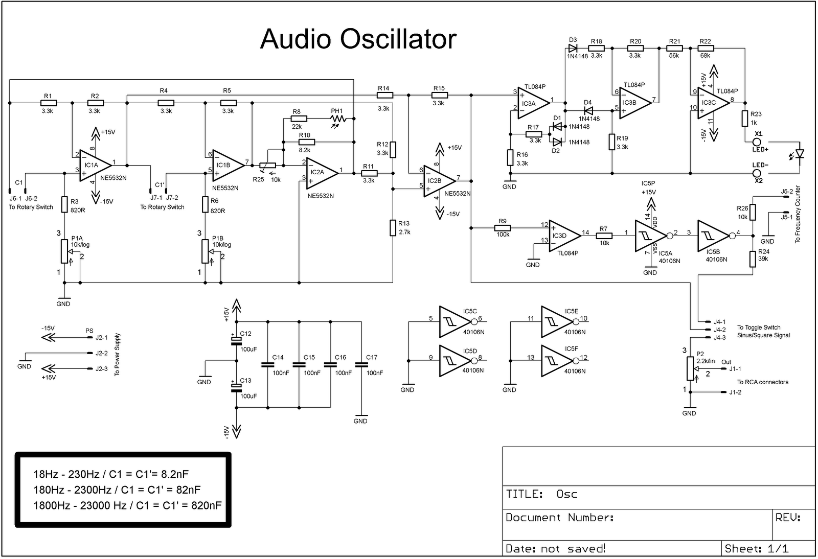
The project involves adding a DIY audio oscillator to a home workshop, which is essential for testing audio projects. While a basic oscillator is already available, it lacks a frequency counter. The design follows a schematic that provides a...
This article continues from the previous one regarding the single character LCD display using an AVR microcontroller. The prior article demonstrated how to display a single letter on an LCD. This article advances the learning process by explaining how...
This preamplifier was designed as a stand-alone portable unit, useful to control the signals generated by guitar pick-ups, particularly the contact "bug" types applied to acoustic instruments. Obviously it can be used with any type of instrument and pick-up....
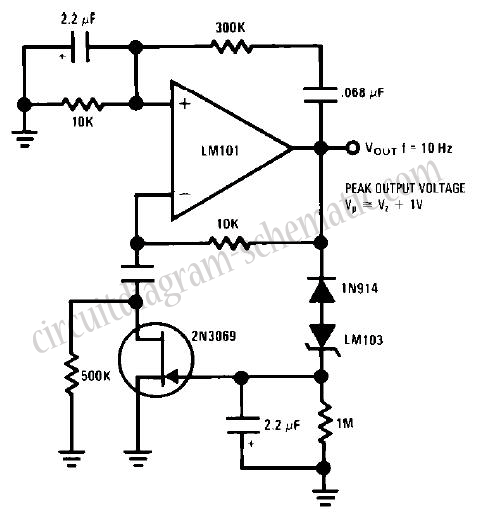
This circuit is a Wien Bridge Sine Wave Oscillator. The primary challenge in generating a low distortion, constant amplitude sine wave is to achieve the appropriate loop gain in the amplifier. By utilizing the 2N3069 JFET as a variable...
The widespread application of Flash technology in microprocessors has led to significant advancements in the development and utilization of one-chip computers. Designers have transitioned from traditional in-circuit emulators (ICE) and JTAG interfaces to more cost-effective and user-friendly development methods....
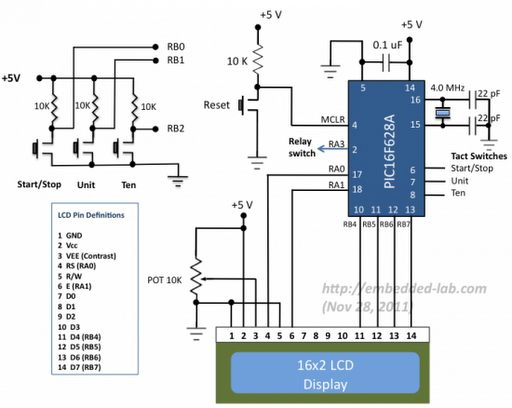
A source code for a simple PIC-based digital timer is provided. The hardware for the project is not available; however, it will be demonstrated using a DIY PIC16F628A breadboard module and I/O board. The complete circuit diagram and firmware...
Warning: include(partials/cookie-banner.php): Failed to open stream: Permission denied in /var/www/html/nextgr/view-circuit.php on line 713
Warning: include(): Failed opening 'partials/cookie-banner.php' for inclusion (include_path='.:/usr/share/php') in /var/www/html/nextgr/view-circuit.php on line 713