
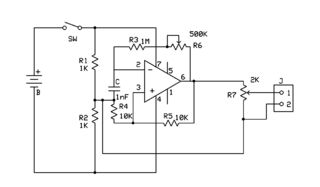
Oscillator keeps THD below 1 ppm
The Wien-bridge sine-wave oscillator circuit is a sophisticated design that leverages the principles of feedback and gain control to produce a stable sine wave output. The absence of a light bulb in this iteration allows for enhancements that improve linearity and reduce harmonic distortion, which are critical for applications requiring high precision, such as testing operational amplifiers and analog-to-digital converters.
The core of the circuit is the Wien-bridge configuration formed by IC1, which acts as both an oscillator and a bandpass filter. This configuration ensures that the generated sine wave maintains a consistent frequency and amplitude. The integration of the voltage-controlled amplifier (VCA) allows for dynamic adjustment of the output amplitude, ensuring stability and reducing the risk of distortion caused by variations in load or supply voltage.
The automatic gain control (AGC) loop, facilitated by diodes D1 and D2, plays a vital role in maintaining output consistency. By rectifying the outputs of IC1 and IC2, the circuit can monitor the amplitude of the output signal and make necessary adjustments in real-time. This feedback mechanism is essential for achieving the desired performance, particularly in high-fidelity applications.
The choice of capacitors is crucial; high-quality film capacitors such as polystyrene or polypropylene are recommended to minimize signal degradation. The specific design of the output stage also addresses non-linearities that can introduce unwanted distortion, further enhancing the circuit's overall performance.
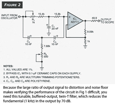
To validate the performance of the oscillator, external filtering is introduced via the twin-T filter. This filter not only attenuates the fundamental frequency but also allows for detailed spectral analysis, enabling precise calculations of total harmonic distortion. Such measurements are essential for ensuring that the oscillator meets the stringent requirements of modern electronic testing applications.
In conclusion, this enhanced Wien-bridge oscillator design represents a significant advancement over traditional configurations, providing a reliable and high-fidelity sine wave output suitable for a wide range of electronic testing scenarios.The Wien-bridge sine-wave oscillator uses a light bulb to stabilize its amplitude. The circuit in Fig 1 doesn`t have a light bulb; it sports several enhancements that lower its distortion and generate a test signal pure enough for testing modern op amps and high-resolution A/D converters. IC1 and associated components form the Wien-bridge and func tion as a bandpass filter. IC1`s output goes to the voltage-controlled amplifier (VCA), IC3. IC3 acts as a "smart resistor" whose value the circuit continuously adjusts via IC4. IC2 adds the outputs of IC1 and the VCA and feeds the result into the bridge. These two op-amp inverters eliminate any common-mode signal that might limit performance. The circuit`s AGC loop begins with diodes D1 and D2. These diodes half-wave rectify the outputs of IC1 and IC2. These outputs are 180 ° out of phase; so IC4 sees a full-wave rectified signal through R1 that is proportional to the output signal`s amplitude. Integrator IC4 compares the average value of the rectified current to a constant current through R2. Any imbalance in these currents causes IC4 to output a correction signal, changing the gain of VCA IC3.
The VCA`s gain adjusts the oscillation`s amplitude until IC4`s input currents are equal. R3 and C3 further filter the correction signal to remove harmonic components that would manifest themselves as distortion at the circuit`s output. D3 minimizes damage to C4 and C7 in the event of reverse polarization. The ac performance of C1 and C2 is critical to this design. I recommend polystyrene or polypropylene film types; and make sure you connect the outside plate as Fig 1 indicates.
Mylar capacitors can degrade the circuit`s performance by 6 dB. C5 and C6 are peculiar to IC1 and IC2. They eliminate distortion arising from VBE nonlinearities in the op amps` output stages. The large ratio of output signal to distortion and noise floor makes verifying the performance of this circuit with standard test equipment difficult. Therefore, I used the tunable, buffered-output, twin-T filter in Fig 2 to reduce the fundamental (1 kHz) in the output by 70 dB.
Spectral analysis of the filter`s output permits calculation of THD. When properly tuned, the filter reduces the second and third harmonics by about 10 and 5 dB, respectively. Harmonic-distortion calculations must take this reduction into account. Harmonic-distortion calculations must factor in the gain of IC1 (Fig 2). Be sure to use the same high-performance capacitors used for C1 and C2 in Fig 1 for C1, C2, and C3 in Fig 2.
🔗 External reference
Related Circuits
International Crystal OF-1 HI oscillator circuit for third-overtone crystals. The circuit does not require inductors. The International Crystal OF-1 HI oscillator circuit is specifically designed to operate with third-overtone crystals, which are capable of generating higher frequency oscillations compared to...
The standard assumption is that the phase shift sections operate independently. According to the equation provided, the loop phase shift reaches -180 degrees when the phase shift of each section is 60 degrees. This condition is met when ω...
The inverter CMOS digital IC CD4049 is utilized to design a square wave oscillator generator. The CD4049 is a hex inverting buffer, which means it contains six independent inverters that can be used to generate square wave signals. This IC...
The generators of square pulses are used in a lot of applications, including the adjustment of conditions of entry in digital circuits and the control of acoustic frequency amplifiers. This circuit is a generator that produces, in combination with...
An attempt has been made to follow an instructable for some time; however, understanding its schematic remains challenging. The issue is not a lack of knowledge regarding the symbols used. In electronic schematics, symbols represent various components and their connections...
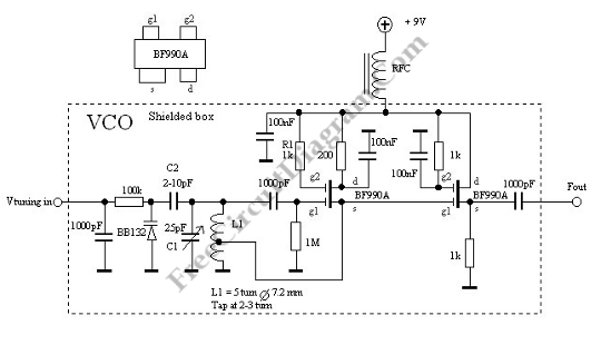
This is a Voltage Controlled Oscillator (VCO) circuit. This circuit is based on a Hartley oscillator. The frequency depends on the values of C1 and L1. The Voltage Controlled Oscillator (VCO) circuit described operates using a Hartley oscillator configuration, which...