
Oscillators
The described circuit components and their interactions form the basis for various applications in electronic systems, particularly in amplification and oscillation scenarios. The coupling capacitor serves as a crucial element in signal transmission, allowing for the passage of AC signals while blocking DC components. The variable resistors provide flexibility in adjusting the circuit's response to input signals, enabling fine-tuning of performance characteristics.
The transistor's biasing arrangements are fundamental to its operation, ensuring that it remains within the active region for amplification. The collector current, influenced by the input audio signal, is critical for driving the connected load, which may include an antenna in RF applications. The RF choke plays an essential role in maintaining the integrity of the power supply by filtering out high-frequency noise, thereby enhancing the stability of the circuit.
In oscillators, the feedback mechanism is vital for sustaining oscillation. The secondary coil's feedback must be appropriately phased to reinforce the oscillation process. The self-biasing feature of the circuit simplifies the design by reducing the need for external biasing components. Additionally, the tuning potentiometer allows for precise frequency adjustments, catering to different operational requirements.
The phase-locked loop (PLL) configuration exemplifies advanced control techniques, where the output frequency is dynamically adjusted to match a reference. This capability is essential in applications such as frequency synthesis and modulation, where precise frequency control is paramount. Overall, the interconnected nature of these components illustrates the complexity and sophistication of modern electronic circuits, highlighting their roles in achieving desired operational outcomes.Those variations, (in effect an alternating signal), will be passed via the coupling capacitor to the next stage - shown by the arrow to the right. We can replace one variable resistor with another. Consider R1 to now be replaced with any one of the devices shown in this following diagram. Each can act as a variable resistor: Other connections mus t be made to the other electrodes of each device to bias it for correct operation so that the input signal can vary the bias which alters the internal resistance of the device, which: in turn varies the voltage at point A, which is passed on through the coupling capacitor to the next stage for further processing. The two resistors connected to the base of this transistor with the resistor in the emitter, form the biasing arrangements.
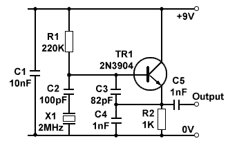
These components set the level of the current flowing through the primary of the transformer - the collector current. An input audio signal is fed via a coupling capacitor to the base of the transistor. This varies the base current which in turn varies the effective resistance of the transistor and hence the collector current.
The circuit below is a typical transmitter radio frequency amplifier. Here the load comprises all the components connected to the collector of the transistor Q1 - C5, L2, etc. and the antenna or whatever is connected to the output. The RF choke RFC2 feeds 12v DC to the device and prevents the RF from getting into the power supply leads.
The input signal provides self-bias to the transistor. The conditions for oscillation are that the level of signal fed back is at an adequate level, and that the signal is in the correct phase to sustain oscillation. This is positive feedback. The feedback is taken by a secondary coil and inserts a signal in the base lead, changing the base-current.
Provided the secondary coil is correctly polarised, the circuit will oscillate. This next diagram shows an audio amplifier (the triangle - with gain in the direction of the arrow) and a feedback network - the collection of resistors and capacitors - a bridged-tee network - connected between the output and the input. This again is a diagrammatic illustration of an audio oscillator. There are many different feedback networks used and they can comprise a wide range of components of all types.
In practice, when first switching on, an oscillator will usually self-start because a burst of noise or a similar transient at the input to the amplifying device is enough for it to commence oscillation. This diagram is also an oscillator. The bottom end of the coil L1 is common to the source and drain current path and transformer action will cause changes in the base current.
This device is self-biasing. A resistor from the collector to the base and from base to earth, together with the emitter resistor, provides some DC bias (base current) for correct operation. When these diodes are reverse-biased, the depletion region between anode and cathode becomes a dielectric whose width is dependent on the applied voltage.
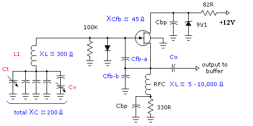
A change of applied voltage changes the width of the dielectric thereby changing the capacitance between anode and cathode. Connected as shown, changing the voltage at the wiper (moving arm) of the manual TUNING potentiometer shown will change the frequency of the oscillator.
The 100k resistor at the junction of the two diodes is to prevent any RF from entering the DC line. This diagram shows the principle of the phase-locked loop (PLL). It consists of a voltage-controlled oscillator which provides the output frequency. That frequency is compared to a reference oscillator using a phase detector or comparator. If we want the output frequency to be the same as the reference oscillator we pass the output frequency through a divide-by-one stage to the phase detector. If the frequencies are not the same, an error voltage proportional to the difference in frequency is produced.
This voltage is filter 🔗 External reference
Related Circuits

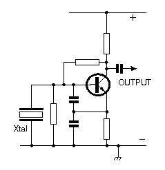
On following pages circuits are shown for 3rd overtone crystals 15 to 65MHz and 5th overtone crystals 60 to 105 MHz operating in their series resonant mode. In both of these circuits with the crystal short circuited, the oscillator...
A question has been raised regarding the type of oscillator found on Wikipedia, specifically referring to the NPN Colpitts oscillator as illustrated in the image titled "File:NPN Colpitts oscillator collector coil.png." The NPN Colpitts oscillator is a type of electronic...
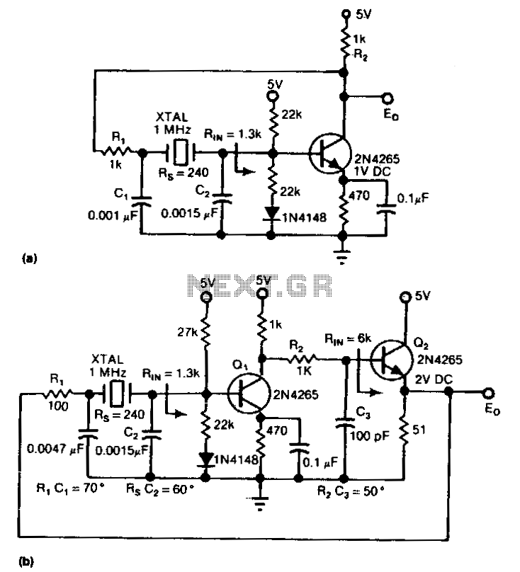
The circuit is an inverter configured as a linear amplifier. By incorporating a crystal and capacitors into the feedback path, the amplifier is transformed into an oscillator, enabling it to oscillate at or near the crystal's resonant frequency. Trimmer...
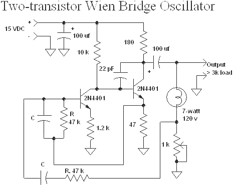
A phase-shift audio oscillator exhibits excellent distortion characteristics due to "softened" diode limiting provided by the 1N914 diode and a resistor divider, along with degenerated gain facilitated by a 68-ohm emitter resistor. To minimize distortion, it is recommended to...
In applications where good frequency stability is essential, such as radio transmitters, basic LC oscillators may not maintain their frequency without drifting. This drift can be caused by small changes in supply voltage, although stabilized power supplies can help...
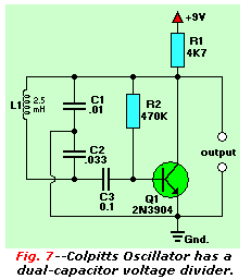
Colpitts oscillators are similar to the shunt-fed Hartley circuit; however, the Colpitts oscillator uses two series capacitors in its LC circuit instead of a tapped inductor. The connection between these two capacitors serves as the center tap for the...
Warning: include(partials/cookie-banner.php): Failed to open stream: Permission denied in /var/www/html/nextgr/view-circuit.php on line 713
Warning: include(): Failed opening 'partials/cookie-banner.php' for inclusion (include_path='.:/usr/share/php') in /var/www/html/nextgr/view-circuit.php on line 713