
Frequency doubler

The described frequency doubler circuit utilizes a 4069 hex inverter IC, which is capable of performing multiple logic operations due to its six inverting gates. The input to the circuit is a square wave signal with a duty cycle close to 50%, which is essential for the proper functioning of the doubler. The voltage level of this input signal must be compatible with CMOS logic levels, typically ranging from 3V to 15V peak-to-peak, depending on the power supply used for the circuit.
The operation begins with the signal being fed into the first inverter (N1), where it is buffered and inverted. The output of N1 is a square wave signal that is 180 degrees out of phase with the input signal. This output is then fed into the second inverter (N2), which inverts the signal again, resulting in a second output that is also 180 degrees out of phase with the first output. The outputs from N1 and N2 are labeled as A and B, respectively.
To generate the necessary spike waveforms for frequency doubling, the outputs A and B are differentiated using capacitors (C1 and C2) and resistors (R1 and R2). This differentiation process generates two spike waveforms, labeled C and D, each 180 degrees out of phase with each other. These spike waveforms are then buffered, inverted, and shaped by the subsequent inverters (N3 and N4), preparing them for combination.
The critical step in frequency doubling occurs when the shaped signals from N3 and N4 are fed into a NOR gate configuration, which consists of diodes (D1 and D2), a resistor (R3), and the fifth inverter (N5). This NOR gate serves to combine the two spike waveforms effectively. The final output of the circuit is obtained by inverting the combined signal with the last inverter (N6), resulting in an output frequency that is twice that of the original input frequency.
The circuit is designed to operate over a broad frequency range, making it versatile for various applications. With the specified component values, the pulse width at the output points E and F is approximately 500 nanoseconds. This leads to a 50% duty cycle output when the input frequency is set at 500 kHz, thereby producing an output frequency of 1 MHz. This characteristic makes the frequency doubler circuit particularly useful in applications requiring frequency multiplication in digital and analog signal processing.This frequency doubler using a single 4069 hex inverter IC, a frequency doubler can be constructed to give an output pulse train whose frequency is twice that of a squarewave input signal. The signal is applied to the input of N1. It should be a squarewave with a duty-cycle of approximately 50% at level compatible with CMOS logic (3-15V peak to peak depending on supply voltage).
The input signal is buffered and inverted by N1, and inverted again by N2, so the outputs A and B of N1 and N2 are squarewave signals 180° out of phase. The output of N1, is differentiated by C1 and R1 and the output of N2 is differentiated by C2 and R2, giving two spike waveforms of C and D, 180° out of phase.
The signals are buffered, inverted and shaped by N3 and N4. These are then combined in a NOR gate consisting of D1, D2, R3 and N5, and finally inverted by N6 to give the frequency twice that of the input signal. The circuit will operate over a wide frequency range. With the component values shown the width of pulses in E and F point is about 500ns, so the duty cycle of the output will be 50% when the frequency is 1MHZ, when the input frequency is 500KHZ.By A.M.
Bosschaert 🔗 External reference
Related Circuits
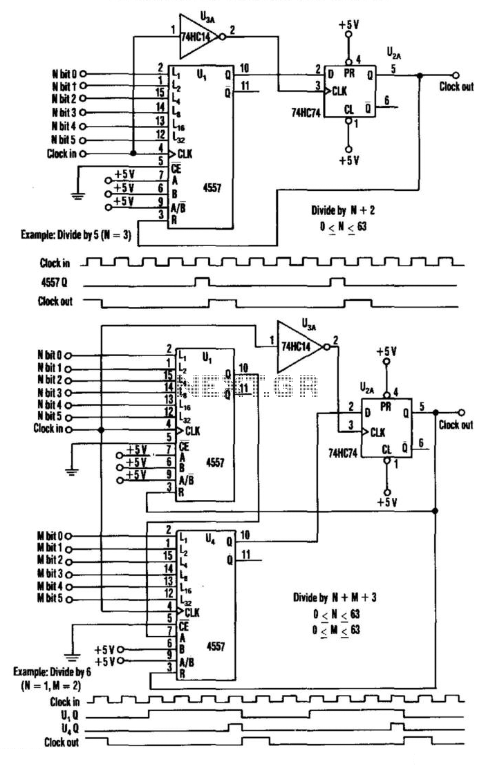
This divider utilizes a variable-length shift register, a type-D flip-flop, and an inverter. The clock signal is connected to the clock input of the flip-flop, while the output of the shift register is connected to the D input of...
A capacitor in series with the crystal may be utilized to adjust the oscillator output frequency. The value may range between 20 pF and 0.01 µF, or it may be a trimmer capacitor, and it will approximately equal the...
The simple circuit does not provide isolation; however, its simplicity, combined with the affordability of sound cards and the protective features added by diodes 1 and 2, makes it suitable for the average user. The physical hardware includes a...
The SE555/NE555 timer was first introduced by Signetics Corporation around 1971. The pin connections and their functions are as follows: Pin 1 (Ground) is the most-negative supply potential and is typically connected to circuit common when powered by positive...
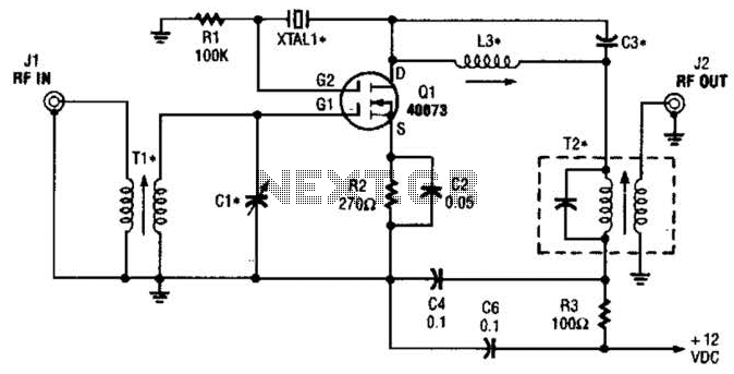
The second gate (G2) of a MOSFET can be utilized to integrate a crystal oscillator within the same stage as a frequency mixer. While this technique is common in tube technology, it is rarely implemented in dual-gate MOSFET circuits....
Designing various electronic circuit systems (synthesizer, modem, decoder, data converter, etc.) often requires a frequency modulator subsystem. An FM modulator is a crucial component in these systems. An FM modulator is an electronic device that encodes information in a carrier...