
Programmable Frequency Divider
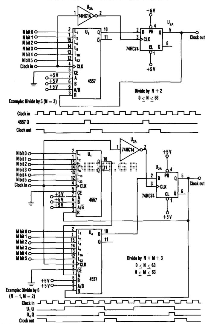
The described circuit operates as a digital frequency divider, leveraging the sequential logic capabilities of a variable-length shift register and a type-D flip-flop. The shift register functions by storing and shifting binary data, while the flip-flop acts as a memory element that captures the state of the shift register output at specific clock intervals.
In this configuration, the clock signal is critical as it dictates the timing of data shifting and state capturing. Each clock pulse initiates a shift in the contents of the shift register, advancing the data stored within it. The feedback mechanism from the flip-flop output to the shift register's reset input ensures that the shifting process is controlled and synchronized with the clock pulses.
The propagation of the "1" through the shift register is essential for the operation of the divider. Once a "1" is introduced, it moves through the register until it reaches the output stage. The subsequent latching of this "1" into the flip-flop occurs at the falling edge of the clock, which enables the system to maintain a stable output state before resetting the shift register.
The reset functionality is a crucial part of the operation, as it allows the shift register to clear its contents and prepare for the next cycle of data input. The timing of the reset is carefully managed; it is only removed after the flip-flop has captured a zero, allowing the cycle to repeat seamlessly.
The divide ratio of (N+2) indicates that the output frequency is reduced relative to the input frequency based on the binary number programmed into the 4557. This programmable aspect allows for flexibility in applications where specific division ratios are required, making this circuit suitable for various digital timing applications and frequency synthesis tasks. Overall, this design effectively combines different digital components to achieve precise frequency division through a well-coordinated sequence of operations. This divider uses a variable-length shift register, a type-D flip-flop, and an inverter. The clock feeds the flip-flop clock input and the output of the shift register feeds the D input of the flip-flop. The FF output is tied back to the reset input of the shift register so that each clock pulse shifts a " " into the 4557. N+1 cycles after the reset pulse is removed. The first "1" will propagate through the register output. The "1" is latched into the FF on the clock"s next falling edge and fed back to the 4557 reset pin, which resets the shift register to zero.
When a zero is clocked into the flip-flop on the next falling clock edge, the reset is removed, restarting the process. The divide ratio is (N+2), where = the binary number that is programmed into 4557. 🔗 External reference
Related Circuits
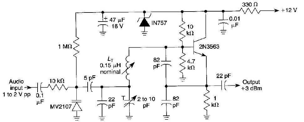
This FM oscillator can be utilized for wireless audio, microphone, and part-15 applications where a stable frequency-modulated oscillator is required. The FM oscillator is an essential component in various communication systems, particularly in wireless audio transmission and microphone applications. It...
A simple technique for measuring frequencies across a wide range with acceptable accuracy limits using a PC is presented. This method follows the basic principle of measuring low frequencies, where the period of a complete wave is measured and...
The master mode selection switch is IC6, which controls the four mode LEDs that correspond to the measured units: kHz, counts, milliseconds, or seconds. In standard frequency counter mode (mode 0, unit: kHz) and counter mode (mode 1, unit:...
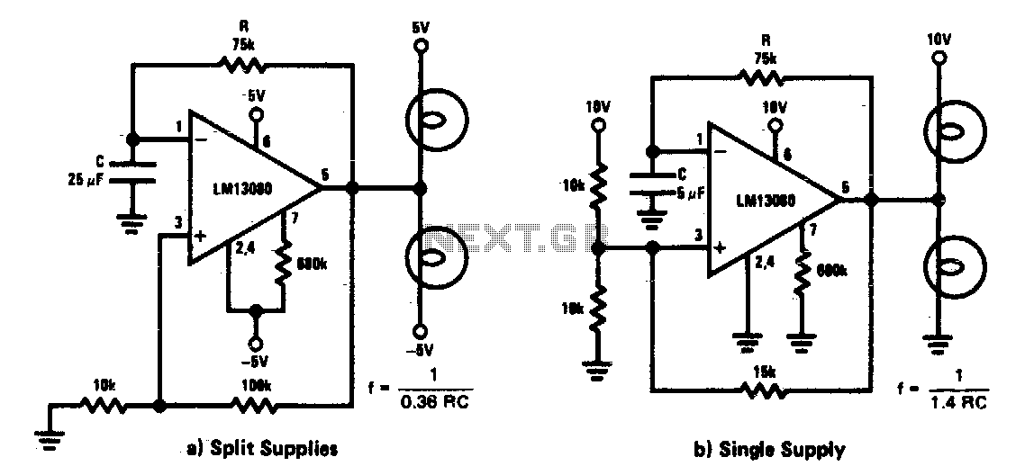
This circuit functions as a low-frequency warning device. The output from the oscillator generates a square wave signal, which is utilized to operate lamps or small relays. The circuit alternately flashes two incandescent lamps. The low-frequency warning device circuit typically...
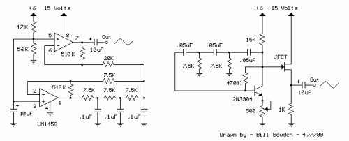
The two circuits demonstrate the generation of low-frequency sine waves by shifting the phase of the signal through an RC network, facilitating oscillation when the total phase shift reaches 360 degrees. The transistor circuit on the right produces a...
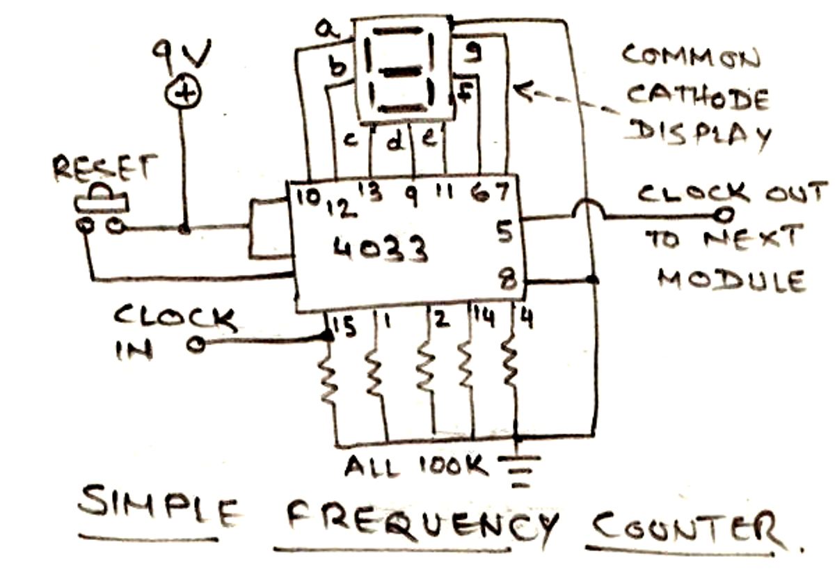
The circuit illustrated below is designed for measuring frequency in Hertz (Hz). It is straightforward to construct, utilizing a single IC 4033 and a common cathode display as the main components. For measuring higher frequencies, typically in the range...