
Oscilloscope Preamp
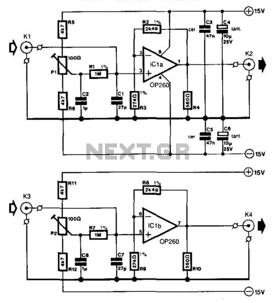
The described circuit employs the OP260 operational amplifier to enhance the sensitivity of an oscilloscope. The choice of a variable gain control allows for fine-tuning the sensitivity range, making it adaptable to various signal levels. The amplifier's design incorporates feedback resistors that significantly influence the gain and frequency response, necessitating careful selection to optimize performance. The importance of maintaining short connections and a common ground is emphasized to minimize noise and ensure stability, which is critical in high-frequency applications.
The circuit's input impedance is set to balance sensitivity and noise performance, with the potential for adjustment to accommodate different probing techniques. The use of presets for DC offset compensation indicates a thoughtful design approach to ensure accurate signal representation. The characteristics of the OP260, including its slew rate and bias currents, inform the design choices and operational parameters, ensuring that the circuit can handle a variety of signal conditions without introducing significant distortion or noise.
Overall, this circuit exemplifies the principles of operational amplifier design in sensitive measurement applications, demonstrating how component selection and circuit layout can significantly impact performance in precision electronics. In many oscilloscopes, the most sensitive range is 2 to 5 mV, although it is often possible to improve this to 1 to 2 m V by a variable gain control. To obtain even better sensitivity, the present preamplifier, which has an amplification of about 10 (20 dB), might be useful. Because most oscilloscopes have a bandwidth of 20 MHz or more, the amplifier must, of course, have a slightly wider bandwidth and that is achieved with a Type OP260 op amp.
This has a slew rate of 550 V7 (is (at an amplification of 10) and a bandwidth of 40 MHz that is virtually independent of the amplification. The gain vs. frequency response is not so good, however: as can be seen from Fig. 39-1 (b), where the characteristics are given for a number of loads. The hump in the curves depends on the value of the feedback resistor, whose optimum value appears to be 2.5 KOhmhm.
The curves in Fig. 39-l(c) accord with different values of R2/R$ for an amplification factor of 10. Some experimentation with the value of R2/Rs for different amplification factors can be instructive. Remember, however, that the output impedance increases from 20 to 225 over the frequency range of 10 MHz to 60 - 70 MHz. It is therefore important to keep all connections on the prototyping board as short as possible and to connect all earth points to a common ground via a separate, heavy track.
Also, do not use an IC socket. An input impedance of 1 was chosen, which results in a fairly high level of noise at the output (with open-circuit input). This value can be reduced, because otherwise the use of a 1:10 probe will be inhibited; it would give constant problems with the noise.
However, when the amplifier is connected to .a suitable source, the noise reduction is normally more than ample to obtain a good trace on the screen. Presets PI and P2 provide compensation for the dc offset and input offset, caused by Rl and R7 respectively.
The input bias current for the noninverting input is about 10 times lower than that for the inverting input, which makes the OP260 more suitable for noninverting circuits. The inverting circuit can also give problems because of the low values of R2 {R%) and R3 (i9). The input bias current is typically 0.2, and the input offset is about 3 mV (max. 7 mV). In this type of circuit, it is important to use a well-regulated power supply. The power-supply suppression up to 10 kHz is roughly 70 dB, and this reduces with increasing frequency.
Any noise or tiny ripple on the supply lines would make the application of the circuit as a small-signal amplifier impossible. The circuit draws a current of about 14 mA. The slew rate, as with most op amps, is asymmetric and might lead to visible distortion of the signal when the drive to the 560- resistor is high at the higher frequencies.
🔗 External reference
Related Circuits
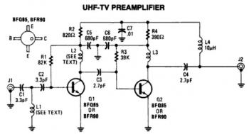
This is a low-cost, antenna-mounted UHF TV pre-amplifier circuit that can provide more than 25 dB of gain. The first stage of the pre-amplifier is biased for optimum gain. L1 and L2 are strip line equivalents with a length...
Application of the differential amplifier circuit in a simple small oscilloscope. The differential amplifier circuit is a crucial component in the design of a simple small oscilloscope. This circuit is designed to amplify the difference between two input voltage signals...
High-quality, discrete component design for input and tone control modules to complement the 60-watt MOSFET audio amplifier with a high-quality preamplifier design. The circuit design focuses on creating a high-fidelity audio preamplifier that enhances the performance of a 60-watt MOSFET...
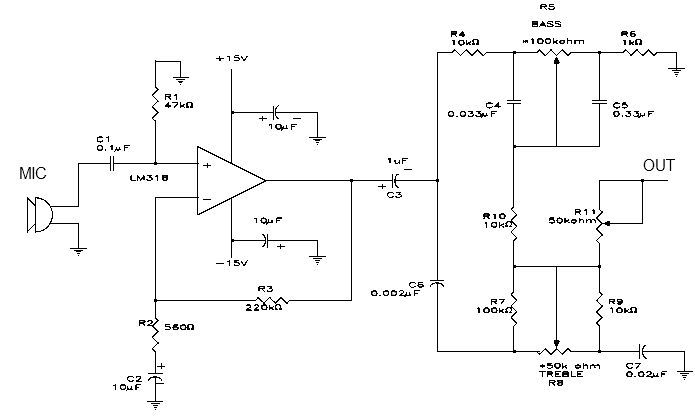
This simple microphone preamplifier is based on the LM318 operational amplifier. The LM318 operates as a standard non-inverting amplifier. Resistor R1 provides a ground input path for the bias current of the non-inverting input. The combination of R2 and...
Contents Introduction Two Versions RF Pickup Component Selection and Noise Sound Photo Gallery Introduction In support of the LM4562 op-amp, National Semiconductor published Application Note AN-1651, which discusses the growing requirements of high-performance audio. The author, Joe Curcio, provided...
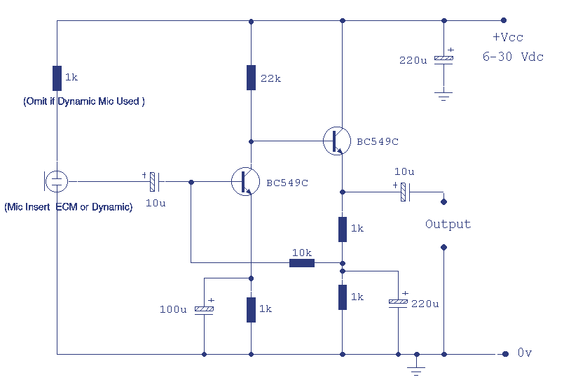
A microphone amplifier that may be used with either Electret Condenser Microphone (ECM) inserts or dynamic inserts, made with discrete components. Both transistors should be low noise types. In the original circuit, BC650C which is an ultra low noise...