
A709 a voltage follower circuit diagram
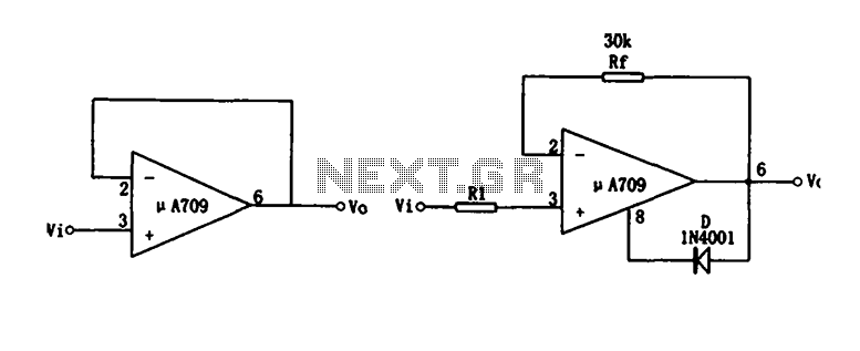
The voltage follower circuit, also known as a unity gain buffer, is characterized by its ability to provide high input impedance and low output impedance. This feature is particularly advantageous in applications where signal integrity must be maintained during transmission, as it prevents loading effects on the preceding stage. The operational amplifier's configuration allows it to replicate the input voltage at the output, ensuring that the output follows the input without amplification.
In practical applications, the voltage follower is frequently used in sensor interfaces, where the signal from a sensor must be buffered before being sent to an analog-to-digital converter (ADC) or further processing stages. The high input impedance ensures that the sensor's output is not significantly affected by the circuit's loading, preserving the accuracy of the measurement.
In the context of the operational amplifier's performance, the stability of the circuit is paramount. The presence of strong negative feedback enhances the linearity and reduces distortion, making the voltage follower suitable for high-fidelity applications. However, care must be taken to avoid conditions that could lead to instability, such as excessive input signal amplitudes that approach the power supply limits of the operational amplifier. In such cases, the circuit may enter a state of saturation, resulting in a loss of linearity and potential distortion of the output signal.
To prevent instability caused by internal oscillations, additional components such as compensating capacitors or resistors may be introduced in the feedback path. These components can help to stabilize the operational amplifier's response, ensuring consistent performance across a range of operating conditions. Additionally, selecting operational amplifiers with suitable bandwidth and slew rate specifications is critical to maintaining the desired performance characteristics in voltage follower applications.Figure (a) shows the circuit as a voltage follower, it is a special case of the in-phase amplifying circuit, the input signal from the integrated operational amplifier with the end of the introduction phase, the feedback resistor is zero, negative feedback is very strong, very stable op amp input impedance great. Output resistance is very small, so this circuit has an impedance conversion function. Impedance transformation means effect the so-called after amplifying a voltage follower, the output voltage is approximately equal to the electromotive force and the output signal source resistance is small.
The circuit is used as an input stage, an intermediate buffer stage and an output stage. The basic relationship of the circuit as follows: Vi + Vis Vo Vo -AVis Where: A-- the open-loop voltage amplification factor; Vis-- pure op amp input voltage; This circuit, when the voltage of the input signal amplitude is increased to nearly the op amps positive supply voltage, the deadlock may occur that will not be the normal output signal, which is due to the positive feedback op amp internal parasitic oscillations produced. In order to prevent this phenomenon, may be employed in Fig (b)
Related Circuits
33 kW and above windlass with Y-conversion power-saving circuit The circuit design for a windlass rated at 33 kW and above incorporates a Y-conversion power-saving mechanism. This design is crucial for optimizing the efficiency of the windlass, which is commonly...
A 100W amplifier with a frequency range from DC to 500KHz features a photoelectric starting operational amplifier with high input impedance and high gain characteristics, enabling transformerless output power of 100W. The load current can reach up to 10A,...
A single-coil latching relay is utilized, which can latch and reset with opposite polarities. Testing of the circuit with dual opposite-biased LEDs showed no flickering in either direction, indicating stable charge and discharge behavior. However, there are concerns regarding...
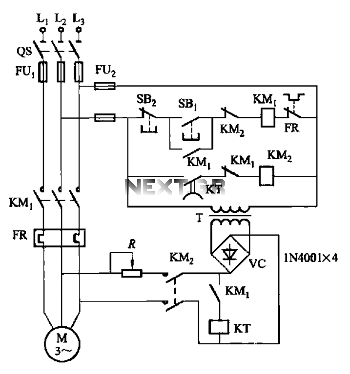
The circuit depicted in Figure 3-134 utilizes an automatic control braking mechanism, which is an enhancement based on the time relay system shown in Figure 3-133 (a). The KT control allows for an adjustable braking time of 2 to...
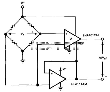
For systems with a single power supply, two operational amplifiers function as instrumentation and buffer amplifiers. The OPA111 AM buffers the reference mode of the bridge and applies that voltage to the reference terminal of the instrumentation amplifiers. The...
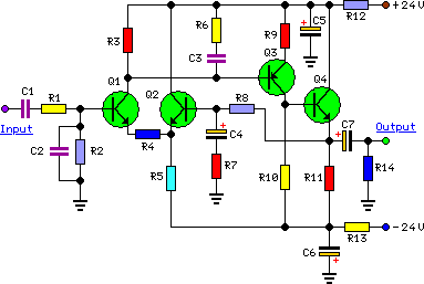
This module utilizes an unconventional topology while retaining the fundamental operational amplifier circuitry of the main module, with some modifications in resistor values. A distinctive feature of this circuit is the incorporation of six-way switches instead of the more...