
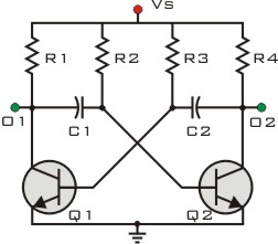
Improved differential circuit diagram

The circuit modification involves integrating the differential circuit with an integrator component, which plays a crucial role in signal processing applications. The integrator is designed to output a voltage that is proportional to the integral of the input signal over time. This is particularly useful in applications where the cumulative effect of a signal is required, such as in analog computing or control systems.
In Figure A1, the integrator is typically implemented using an operational amplifier (op-amp) configured in an inverting mode. The input signal is applied to the inverting terminal of the op-amp through a resistor, while a capacitor is connected between the output and the inverting terminal, forming a feedback loop. The non-inverting terminal is grounded.
The output voltage of the integrator can be expressed mathematically as V_out(t) = -(1/RC) ∫ V_in(t) dt, where R is the resistance, C is the capacitance, and V_in(t) is the input voltage. This equation indicates that the output voltage is the negative integral of the input voltage, scaled by the time constant RC of the circuit.
Additionally, it is essential to consider the frequency response of the integrator, as it can significantly influence the performance of the overall differential circuit. The integrator will have a high gain at low frequencies and will attenuate high-frequency signals, which can lead to phase shifts and potential instability in certain applications. Therefore, proper selection of the resistor and capacitor values is critical to ensure that the integrator operates effectively within the desired frequency range.
Overall, the integration of the differential circuit with an integrator enhances its functionality, enabling it to process signals that require accumulation over time, thereby expanding the potential applications in various electronic systems. As shown for the modification of the differential circuit. Figure, A1 is an integrator, the output is
Related Circuits
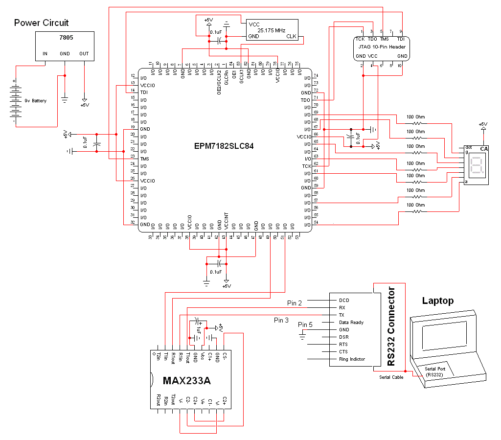
The schematic for this project is a modified version of the CPLD development board schematic. Several new components have been added for this project, and the completed schematic can be viewed below. The main components in the schematic are...
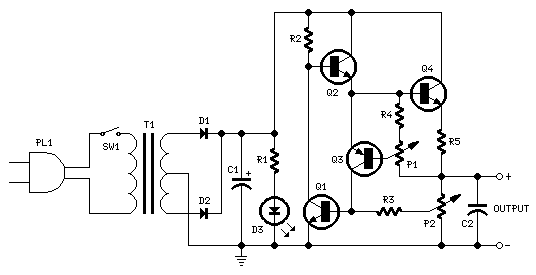
A Variable DC Power Supply is an essential tool for electronics hobbyists. This circuit is not entirely new, but it is simple, reliable, robust, and short-proof, offering variable voltage up to 24V and variable current limiting up to 2A....
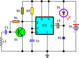
This circuit is designed to detect incoming calls on a cellular phone, even when the phone's ringer is turned off, by utilizing a flashing LED. The device should be positioned a few centimeters away from the cellular phone, allowing...
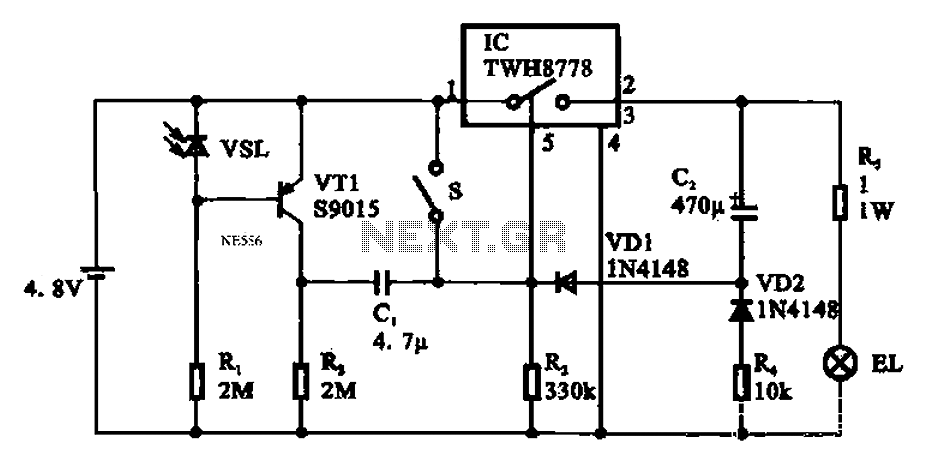
Automatic emergency lamp circuit featuring an electronic switch integrated circuit. This circuit is designed for automatic emergency lighting. The system operates based on ambient light conditions; when light levels are low at night, the circuit activates the emergency lamp....
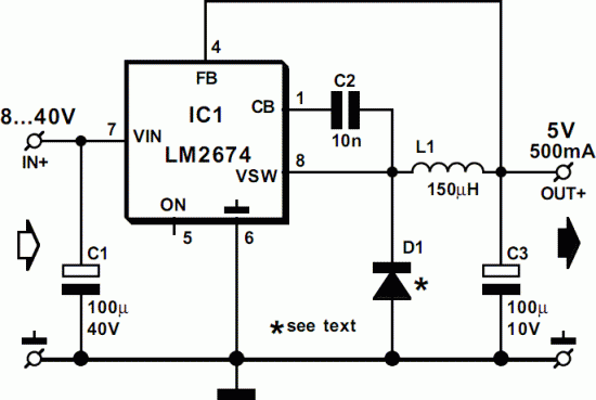
This 5-volt Switch Mode Power Supply circuit utilizes an integrated circuit (IC) from National Semiconductor, which specializes in the production and design of ICs for switch-mode power supply applications. The 5-volt Switch Mode Power Supply (SMPS) circuit is designed to...
This circuit is designed to drive a relay coil using a low power output, typically from an integrated circuit (IC) such as a 555 timer or a TTL/CMOS device. It facilitates the switching of high loads or loads requiring...