
OTL transistor radio in a power amplifier circuit
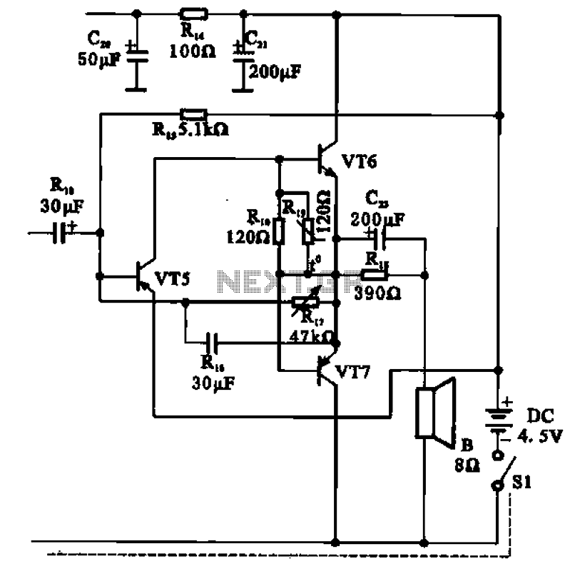
The described circuit is a common output transformerless (OTL) power amplifier, which is designed to drive speakers directly without the need for an output transformer. This configuration is particularly beneficial in radio applications where space and weight are critical. The use of germanium transistors, such as VT6 (NPN) and VT7 (PNP), allows for lower voltage operation and improved thermal stability compared to silicon counterparts, making them suitable for low-power applications.
In this design, the driver stage is established by the VT5 bias resistor, which sets the operating point for the amplifier stages. The complementary symmetry arrangement of VT6 and VT7 ensures that both halves of the audio signal are amplified, improving linearity and reducing distortion. This is achieved by having the NPN and PNP transistors work in tandem, with VT6 amplifying the positive half of the waveform and VT7 handling the negative half.
The biasing resistor plays a crucial role in maintaining the correct biasing conditions for the transistors, ensuring that they operate in their active regions during signal amplification. The omission of certain details related to the bias resistor and incentives suggests a focus on the primary function of the circuit rather than its complete operational nuances.
Overall, this OTL amplifier circuit exemplifies an efficient and compact design suitable for portable transistor radios, where high performance and low power consumption are paramount.Transistor radio shows common OTL power amplifier circuit, VT5 bias resistor driver stage. VT6 and VT7 is a pair of complementary symmetry tube. VT6 germanium material NPN transistor, VT7 is germanium PNP transistor. VT6, VT7 and the biasing resistor composition typical OTL amplifier. To illustrate the process of the circuit, circle omitted satin bias resistor and incentives.
Related Circuits
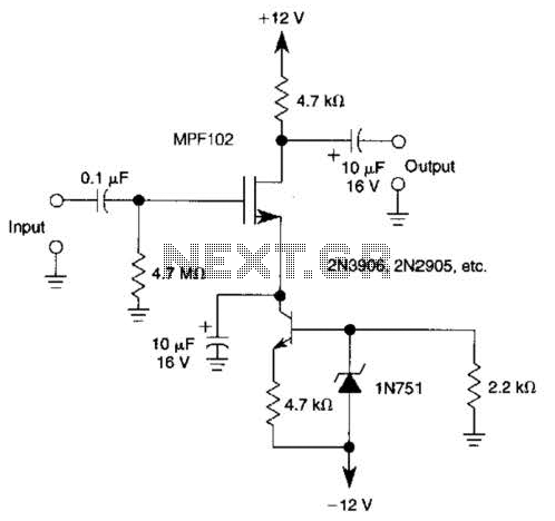
A current source (MPF102) in the source lead of the bipolar transistor 2N3906 allows for precise control of drain current. The circuit incorporates an MPF102 JFET configured as a current source, which is connected to the source terminal of a...
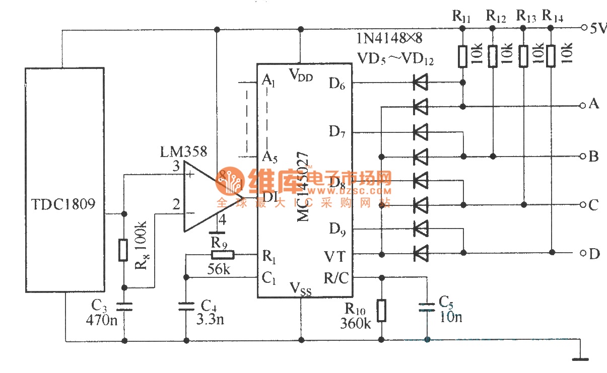
The TDC1808/TDC1809 is a pair of wireless remote control transmitter and receiver components. They utilize an internal antenna to transmit both digital and analog signals. These components are suitable for various wireless remote control devices. Key features include compact...
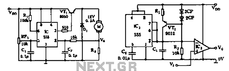
The circuit consists of a 555 motor automatic governor configuration. It includes flip-flops, a 555 timer, and a switching tube. A sampling circuit is formed by connecting R7 and the motor in series. RP1 is used to control the...
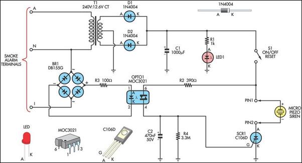
This alarm circuit is designed to monitor a mains-powered smoke detector located in a shed used for dog kennels. It ensures complete isolation from the mains, allowing low-voltage (12V) cabling to connect to the alarm circuit situated inside the...
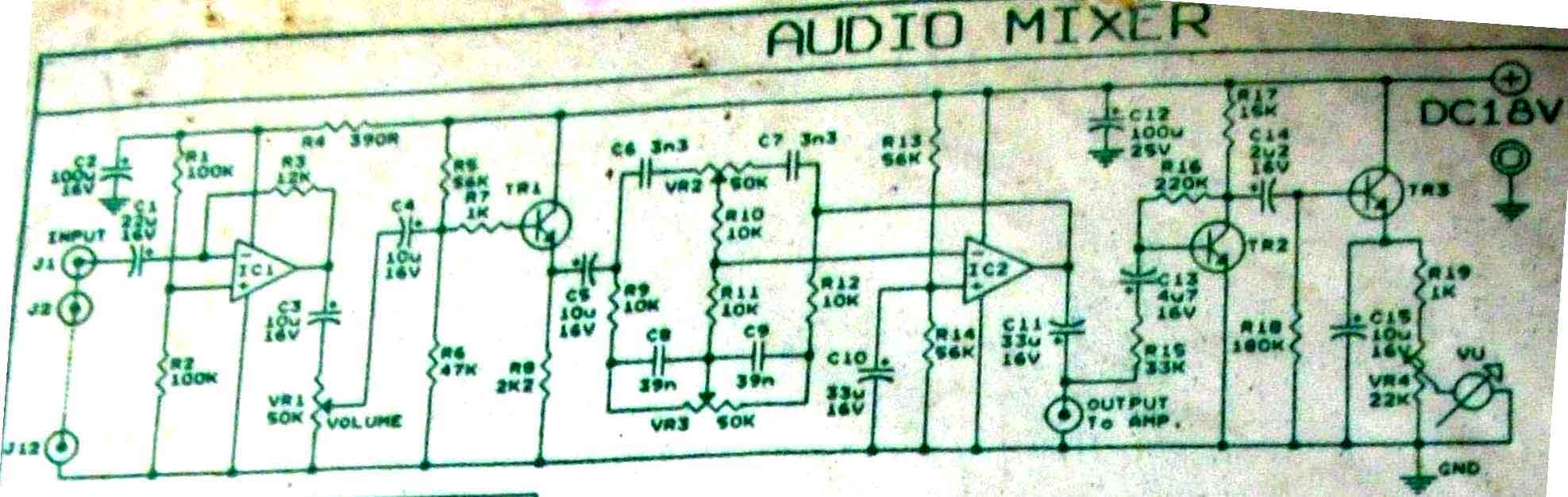
This is audio mixer circuit. The circuit is for one channel input, if you need, for example 5 channel mixer, then you need to build 5 similar circuits. The audio mixer circuit described is designed to handle a single channel...

The transmitter's function is to modulate the original signal frequency of the message-carrying signal, a process known as modulation. The circuit realization of this function is referred to as a frequency modulation (FM) circuit. FM tuners are categorized into...