
Peak detector

The CA3130 BiMOS operational amplifier is a versatile component that combines the advantages of both bipolar and CMOS technologies. Its unique design allows it to operate effectively in a variety of applications, particularly in circuits requiring high-speed performance and low noise. The CA3130 is characterized by its ability to handle large-signal inputs, making it suitable for use in peak detection circuits, signal conditioning, and other high-frequency applications.
In a typical configuration involving peak detection, the peak-positive circuit utilizes the high bandwidth of the CA3130 to quickly respond to positive signal peaks. Conversely, the peak-negative circuit, while still functional, exhibits reduced bandwidth due to the inherent limitations imposed by the second stage of the amplifier. This reduction in bandwidth can affect the circuit's response time and accuracy in detecting negative signal peaks.
To optimize performance, careful consideration should be given to the design parameters of the circuit, including feedback components, input impedance, and power supply levels. The use of appropriate filtering techniques may also help mitigate bandwidth limitations, ensuring that the circuit can effectively handle the desired frequency range.
Overall, the CA3130 BiMOS op amp is a powerful tool for engineers looking to implement high-performance circuits, particularly in applications where signal integrity and response time are critical.Circuits are easily implemented using the CA3130 BiMOS op amp. For large-signal inputs the bandwidth of the peak-negative circuit is less than that of the peak-positive circuit. The second stage of the CA3130 limits bandwidth in this case.
Related Circuits
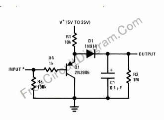
Using only a single transistor and a few passive components, a fairly sensitive peak detector circuit can be built. This peak detector circuit is suitable for various applications. The peak detector circuit utilizes a single transistor, typically configured in a...
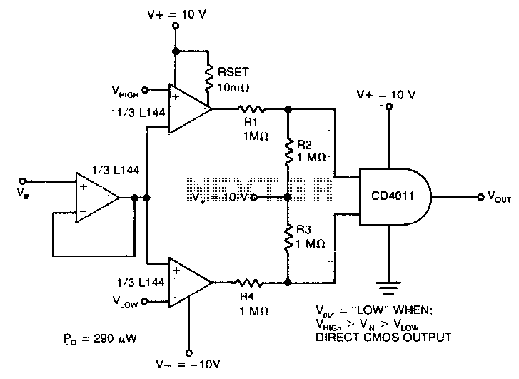
The detector utilizes three sections of an L144 and a DC4011 type CMOS NAND gate to create a very low power voltage monitor. If the input voltage, Vin, is above Vhigh or below Vlow, the output will be a...
This circuit can be constructed using easily accessible, low-cost components, some of which might even be found in a collection of spare parts. The circuit in question is designed to utilize common electronic components, making it an ideal project for...
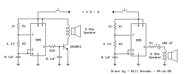
This is a basic 555 square wave oscillator used to produce a 1 kHz tone from an 8-ohm speaker. In the circuit on the left, the speaker is isolated from the oscillator by an NPN medium power transistor, which...
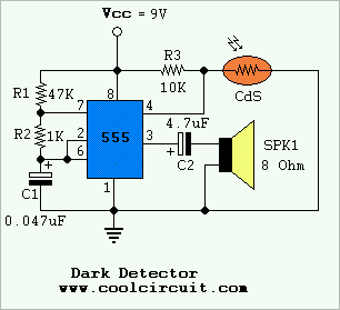
Dark Detector with LM555. This is a dark detector circuit that generates sound in the absence of a light source and remains silent when light falls on the CdS (Cadmium Sulfide) sensor. The dark detector circuit utilizes the LM555 timer...
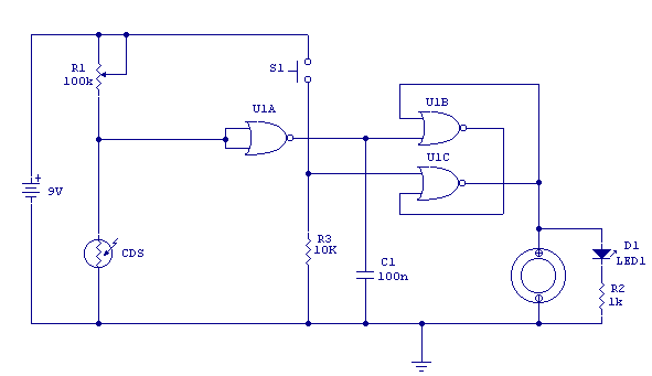
Variable resistor R1 adjusts the light threshold at which the circuit triggers. R1's value is chosen to match the photocell's resistance at darkness. The circuit uses a CMOS 4001 IC. Gate U1a acts as the trigger, U1b and c...