
PLL FM Transmitter Circuit
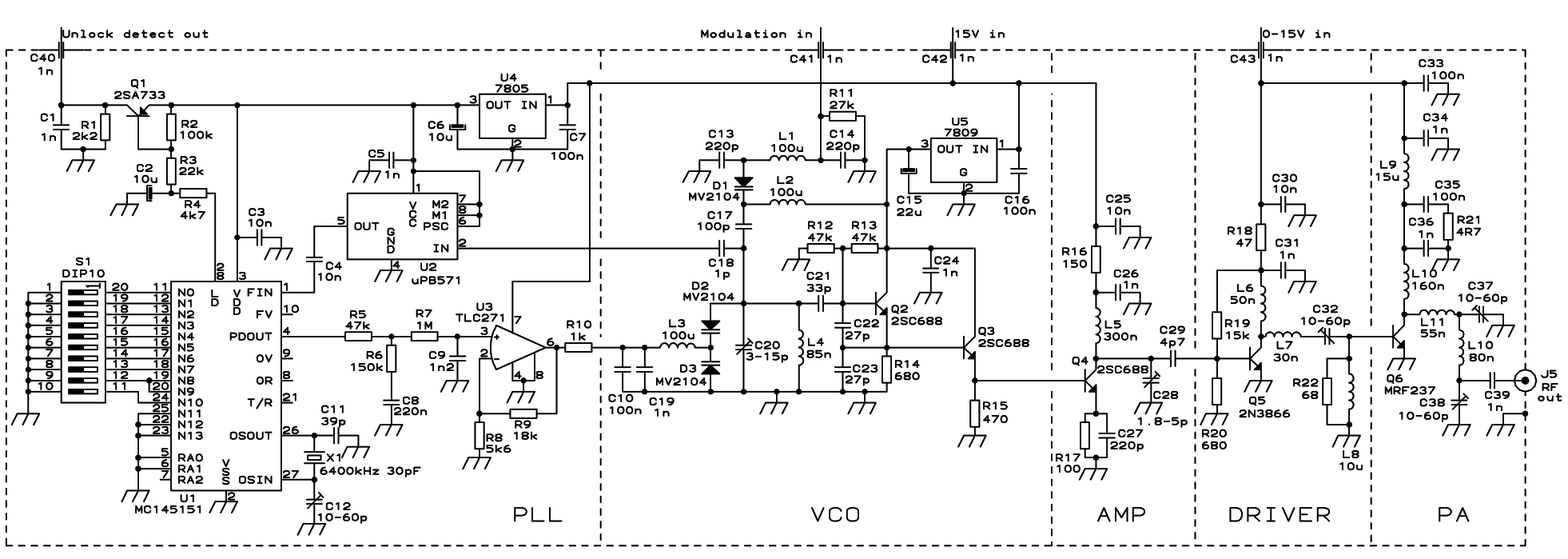
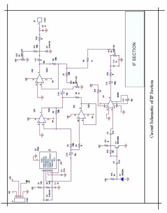
The PLL transmitter exciter is a sophisticated device designed for RF applications, leveraging a phase-locked loop (PLL) architecture to ensure frequency stability and low noise operation. The MC145151 PLL frequency synthesizer forms the core of this exciter, enabling precise frequency selection in 100 kHz increments across the FM band. The integration of a Colpitts VCO, powered by a regulated 9V supply, enhances the performance by utilizing varactor diodes for frequency control, which significantly reduces phase noise and improves overall signal integrity.
The output stage of the exciter is meticulously designed, incorporating an emitter follower buffer to isolate the VCO from subsequent amplification stages. The class A amplifier provides initial signal amplification, followed by a class B driver that further boosts the output before it reaches the class C power amplifier. This multi-stage amplification approach, combined with medium-Q tuned impedance matching networks, ensures that the output power can be finely controlled from zero to 4 watts by adjusting the supply voltage, thereby allowing for versatile applications in low-power transmission.
To ensure operational reliability, the PLL unlock detector serves as a critical safety feature, automatically shutting down the transmitter in the event of a frequency lock failure or other malfunctions. The design also considers the necessity of harmonic filtering, emphasizing that direct connection to an antenna is not advisable without additional filtering components to prevent signal distortion and interference.
The double-sided PCB layout is optimized for performance, with a dedicated ground plane to minimize noise and enhance signal integrity. The careful arrangement of components and the inclusion of soldered shields contribute to reducing electromagnetic interference (EMI) between stages. The design process for programming the frequency utilizes a binary switch configuration, allowing for straightforward frequency adjustments through user-friendly controls.
In conclusion, the PLL transmitter exciter represents a robust solution for RF signal generation, offering precise frequency control, adjustable output power, and built-in safety features, making it suitable for a variety of applications in wireless communication systems.The PLL transmitter exciter has the functions of providing a stable, low noise, frequency-selectable RF signal and amplify it to a controllable output power sufficient to drive the power amplifier. It uses a PLL frequency synthesizer built with MC145151, which covers the FM band in 100kHz steps. The VCO covers only a few MHz without readjustment. The pll transmitter output power is controllable from zero to 4 watts. A PLL unlock detector is included, to shut down the transmitter in the event of a malfunction. The Colpitts VCO is powered from a local 9V regulator, and has the frequency controlled by two back-to-back varactors, resulting in minimal loading and thus ultra low phase noise. The output of the VCO goes through an emitter follower buffer stage, then through a broadly tuned class A amplifier, followed by a class B driver and a class C power amplifier, which use medium-Q tuned impedance matching networks.
These last two stages are powered from a separate input, so that the output power of the Phase-Locked Loop transmitter can be controlled from zero to 4 W by adjusting this voltage from zero to 15V. Note that the output of this pll module does not have enough harmonic filtering to connect it directly to an antenna.
If you want to use this exciter as a stand-alone low power transmitter, you should add a low pass filter. The Phase-Locked Loop transmitter is built on a double sided PCB, which has its top side copper left mostly undisturbed as a ground plane.
The copper is removed only around non-grounded pins. The ground connections are soldered on the top side, so it`s not necessary to have plated-through holes. This drawing shows the two sides of the PCB, so that you can print it and fold it in the middle to see how the two parts align.
You will have to invert the image to print it for making the board, so that the ink gets in contact with the copper. This PCB is fitted with soldered shields all around and between stages, on both sides of the board. They are best installed before populating it. First you set all trimmers to mid range and program the frequency. For this task, you simply add the switch weights: The least significant switch produces 100kHz, the second adds 200kHz, the next 400kHz, and so on, until the eighth, which adds 12.
8 MHz. The ninth actually connects to two inputs of the PLL chip, so it adds 76. 8 MHz, with the tenth switch adding 102. 4MHz. To calculate switch settings for a given frequency, you simply decompose it into its binary components, and set the proper switches. Note that a switch that is ON is NOT adding its frequency contribution! For example, if you want to transmit on 96. 5 MHz, you would set switches 9, 8, 7, 3, and 1 to OFF, the others to ON. Now you should connect a 15V power supply to the main power input only, with a voltmeter at the output of U3, and a frequency counter at the collector of Q4.
If you get the correct frequency, you are in big luck and should go and play lottery! Usually the VCO will be out of capture range. If the voltmeter reads around 14V, it means the frequency is too low. If it reads close to zero, it means the frequency is too high. The frequency counter should agree with this. You need to adjust the VCO center frequency to bring it into range. For this task you have two adjustment points: One is C20, the other is bending L4! Usually the trimmer alone does not give enough range, so feel free to bend the coil. When you have adjusted the VCO roughly right, the PLL will lock in, and you will get a stable output frequency, very close to the one you want. Adjust L4 and C20 so that the voltmeter reads roughly 9V. Such a relatively high varactor voltage is convenient for best noise performance, because it keeps the varactors from entering conduction at the RF peaks.
Ideally you should adjust the coil so that the trimmer is near center range with the voltage at 9V. This gives you easiest correction later 🔗 External reference
Related Circuits
A clock-and-data recovery (CDR) circuit is utilized to recover the clock from a transmitted data stream and re-time that data with the recovered clock. These circuits are generally positioned at the front-end of receiver chips to extract the clock...
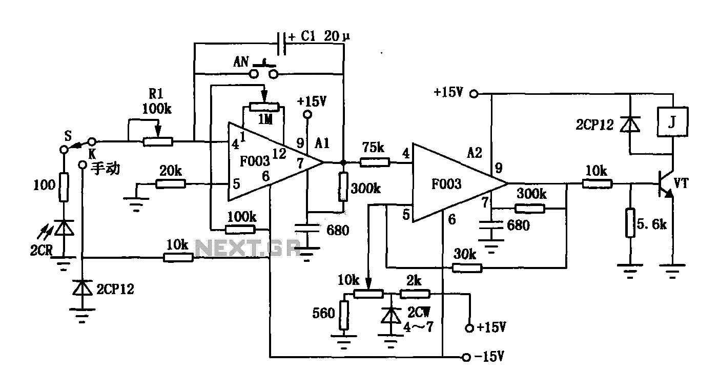
The F003 circuit is a versatile photographic component that functions as an operational amplifier amplifying automatic timer circuit. The operational amplifier A1 serves as an integrator, while operational amplifier A2 is configured as a comparator. A 2CR silicon photocell...
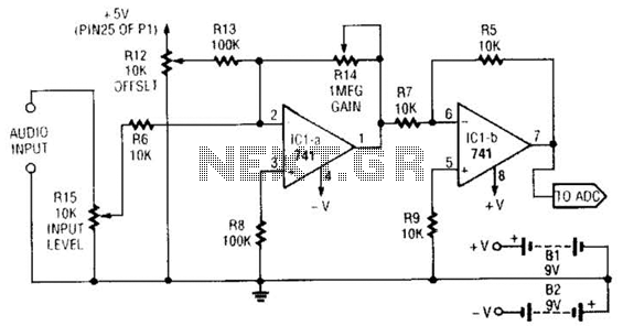
This simple general-purpose driver for an analog/digital converter uses two 741 IC devices with adjustable gain and offset. Other op-amps might be substituted, but some circuit adjustments might be needed. The circuit consists of two operational amplifiers (op-amps) from the...

This circuit was designed to control power delivery to a Peltier cooler in a vehicle. The power to the load from the vehicle's battery is managed by a Single Pole Double Throw (SPDT) relay. The circuit utilizes an SPDT relay...
Obtain more information about the circuit diagram of a mobile jammer by visiting this link. A GSM jammer, or cell phone jammer, is a device that transmits signals on the same frequency used by the GSM system. The effectiveness...
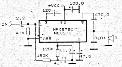
An amplifier circuit is particularly well-suited for use in confined spaces, such as within vehicles. It requires a voltage supply ranging from 9 Volts to a maximum of 17 Volts. This amplifier circuit utilizes the IC MPC575C, which is...
Warning: include(partials/cookie-banner.php): Failed to open stream: Permission denied in /var/www/html/nextgr/view-circuit.php on line 713
Warning: include(): Failed opening 'partials/cookie-banner.php' for inclusion (include_path='.:/usr/share/php') in /var/www/html/nextgr/view-circuit.php on line 713