
Power Factor Correction (PFC) Circuit Reduces MOSFET Miller Effect
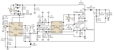
In a cascode configuration, the upper MOSFET is typically subject to the Miller effect, which can lead to increased switching losses and reduced efficiency. By incorporating a discharge path for the upper MOSFET, the gate capacitance can be effectively managed. This modification allows for faster turn-off times and mitigates the impact of voltage transients, which are particularly pronounced due to the Miller capacitance.
The discharge path can be implemented using a resistor or an additional transistor that provides a controlled discharge route for the gate capacitance when the MOSFET is turned off. This approach ensures that the gate voltage is lowered more quickly, thereby reducing the time the MOSFET remains in the linear region during switching transitions. As a result, the overall switching losses are minimized, which is crucial for applications requiring high efficiency, such as in power supply designs focused on PFC.
Furthermore, improving the PFC performance not only enhances the efficiency of the power supply but also helps in meeting regulatory standards for harmonic distortion and energy consumption. This modification can lead to a more robust design that is capable of handling varying load conditions while maintaining optimal performance. The integration of a discharge path into the upper MOSFET of a cascode circuit exemplifies an effective strategy for advancing the operational characteristics of modern power electronics.By adding a discharge path to the upper MOSFET of a cascode circuit, the unavoidable Miller effect is greatly reduced and the PFC performance of a power supply`s front end can be improved 🔗 External reference
Related Circuits
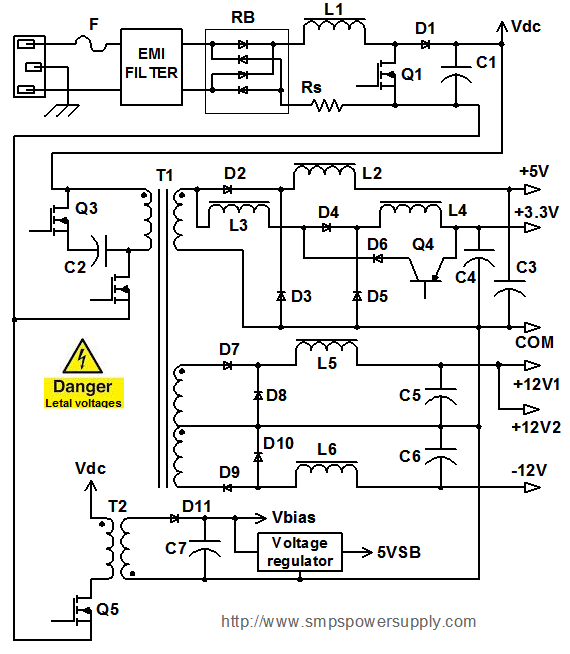
All electronic systems and equipment, regardless of their size or function, share a common requirement: a power supply unit (PSU) that converts input voltage into suitable voltage levels for their circuits. The most prevalent type of PSU today is...

The logic diagram of the CD4538BC Dual Precision Monostable is shown in the following schematic diagram. This IC is a dual, precision monostable multivibrator with independent trigger and controls, according to the datasheet. This CD4538BC IC features a wide...
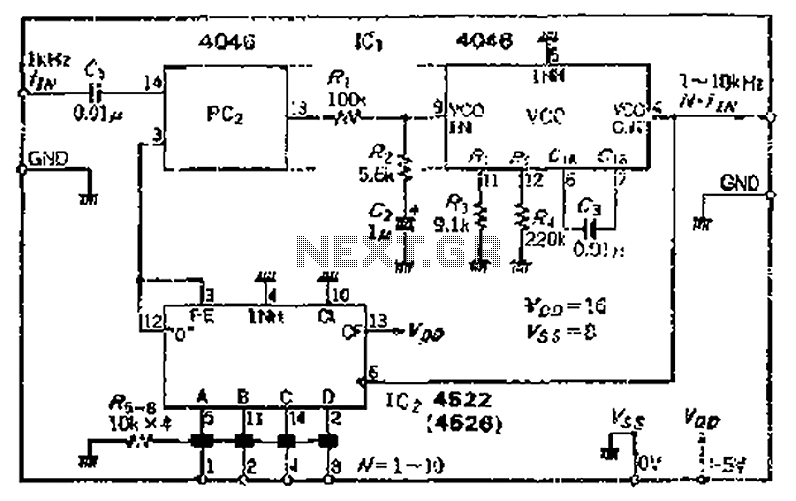
The CMOS IC 4046 Phase-Locked Loop (PLL) operates with a maximum frequency of 1 MHz. It is connected to a programmable divider, allowing it to process input frequencies. As the frequency increases by a factor of t, the circuit's...
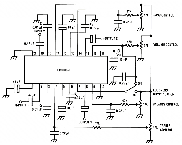
The LM1036 is a DC-controlled circuit designed for tone (bass/treble), volume, and balance adjustments in stereo applications, including car radios, televisions, and audio systems. It features an additional control input for easy loudness compensation. The circuit includes four control...
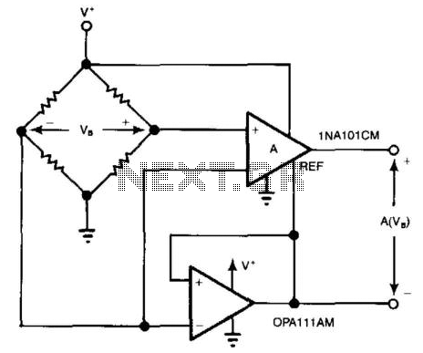
For systems with a single power supply, two operational amplifiers function as instrumentation and buffer amplifiers. The OPA111 AM buffers the reference mode of the bridge and applies that voltage to the reference terminal of the instrumentation amplifiers. The...
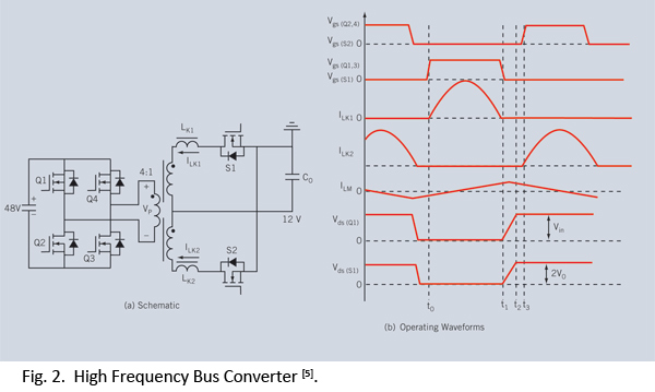
Distributed power systems are commonly used in telecommunications, networking, and high-end server applications, utilizing a 48 V bus voltage derived from the telecom industry. This 48 V bus supplies several isolated point-of-load (POL) converters that power the end loads,...