
Power-Saving Intermittent Converter
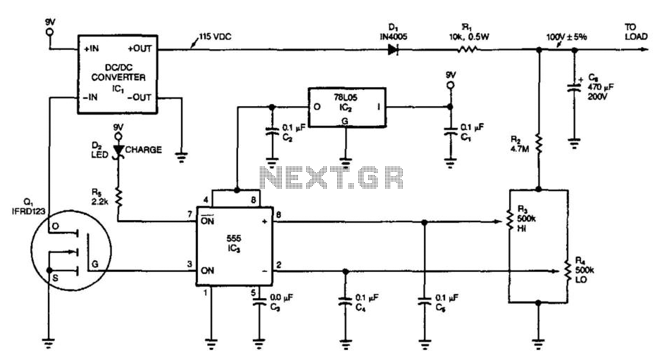
This circuit features a DC/DC converter that efficiently manages power by utilizing a 555 timer as a dual-limit comparator. The primary function of the circuit is to maintain the operation of the DC/DC converter only when necessary, thereby optimizing energy use. The 555 timer monitors the voltage across the filter capacitor, C6, which acts as an energy reservoir. The output from the timer drives a field-effect transistor (FET), Q1, which controls the converter's operation.
The converter is designed to step up a low input voltage of 9 Vdc to a higher output voltage of 115 Vdc, making it suitable for various applications that require high voltage from a low voltage source. The voltage across C6 is critical for determining the operational state of the circuit. The resistor R3 sets the upper threshold for the voltage level that must be reached before the converter is turned off. This feature prevents overcharging of the capacitor and ensures that it provides adequate energy to the load without exceeding its capacity.
The voltage divider formed by resistors R2, R3, and R4, along with the diode D1, plays a crucial role in managing the discharge of C6, allowing the load to draw power while preventing backflow when the capacitor voltage drops. The 555 timer re-engages the converter when the voltage across C6 falls below a third of the supply voltage (Vcc), ensuring that the load receives power as needed.
The circuit's design allows for significant power savings, particularly in applications where the load may not be continuously active. The duty cycle of 5 seconds on and 150 seconds off results in a substantial reduction in average power consumption. Additionally, by substituting the standard 555 timer and linear regulator with CMOS alternatives, further efficiency can be achieved, making the circuit suitable for battery-operated devices or energy-sensitive applications. This design exemplifies effective power management and energy conservation in electronic circuits. This circuit switches its dc/dc converter, IC1, off whenever the large filter capacitor, C6, has suffic ient charge to power the load. This particular circuit uses a dc/dc converter that produces 115 Vdc from, a 9-Vdc input; you can tailor the circuit to suit other converters. The heart of the circuit is a 555 timer configured as a dual-limit comparator. Thus, the 555 turns the converter on or off, depending on the voltage across C6. The 555"s complementary output lights the charge LED when the FET is on. Initially, the voltage on C6 is zero, and the 555"s output turns on the FET, Ql, in turn, enabling the converter to run, which charges C6.
When the voltage on the capacitor reaches the value set by R3, the 555 turns the converter off. Then, C6 slowly discharges into the combined load of the voltage divider (R2, R3, and R4) and the reverse-biased blocking diode, Dl. When the voltage falls below 1/3 Vcc, the 555 restarts the dc/dc converter. If this circuit powers a load that periodically goes into a zero-power, shutdown mode, the 555 switches the dc/dc converter on full time whenever the load kicks in.
When the supply voltage falls below 7.5 V, the output of the converter is no longer high enough to charge, the LED doesn"t light. The circuit uses 205 mA when the converter is on and 10 mA when the converter is off. The duty cycle comprises a 5-s on period, a 150-s off period, and it represents a 92% power reduction.
You can further reduce power consumption by removing the charge LED and using a CMOS 555 and a CMOS 78L05 regulator. 🔗 External reference
Related Circuits
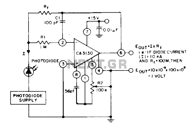
The circuit utilizes three CA3130 BiMOS operational amplifiers in an application that is sensitive to sub-picoampere input currents. It provides a ground-referenced output voltage that is proportional to the input current flowing through the photodiode. The circuit design employs three...
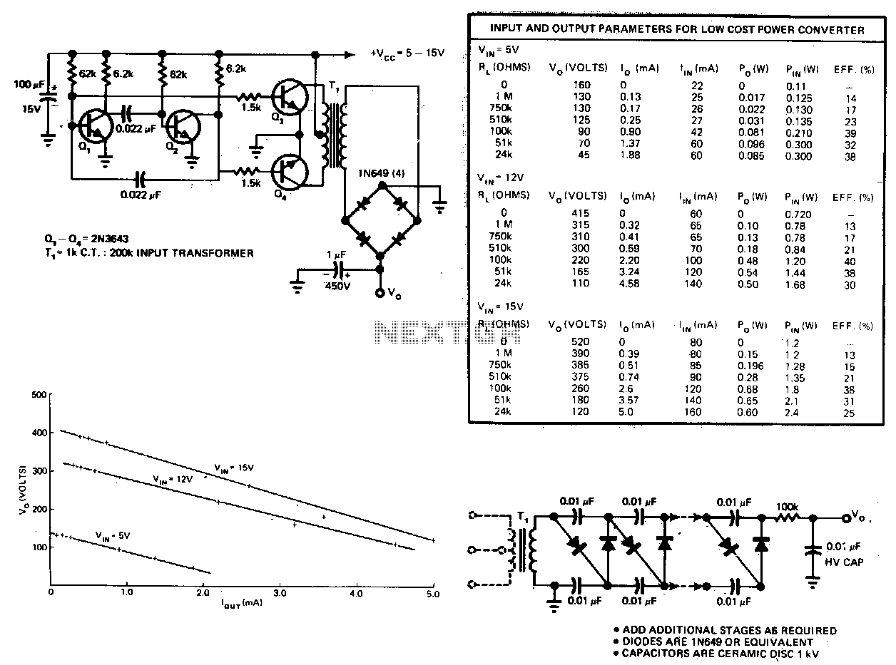
This low-power converter supplies approximately 100 mW of DC power to a load and is useful for isolating or deriving DC voltages. It operates at a frequency of around 200 kHz. The inductor is wound on a 22-mm diameter,...
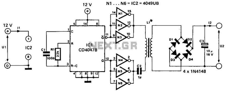
This circuit consists of an astable multivibrator driving a push-pull pair of transistors into the transformer primary. The multivibrator frequency should equal around 1 or 2 kHz. For higher DC voltages, voltage multipliers on the secondary circuit have been...
The result displayed on the LCD is incorrect; the thermometer shows a reading of 414 degrees instead of the actual room temperature. Assistance is needed to determine whether the issue lies within the hex file or the sensor itself....
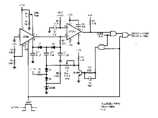
The simple 4-digit converter circuit has an output count of 1, designed to operate within a frequency range of f-IMHz to 10.000. All diodes used in the circuit are IN4146, and the capacitors are made of `POLYSTYRENE` NPO. The...
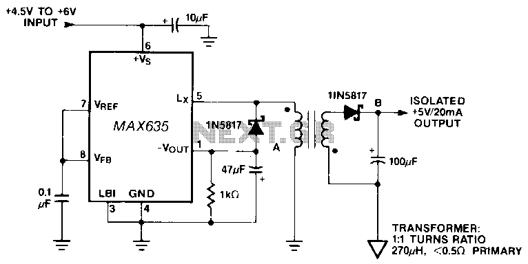
In this circuit, a negative output voltage DC-DC converter generates a -5 V output at pin A. To achieve -5 V at point A, the primary of the transformer must fly back to a diode drop that is more...
Warning: include(partials/cookie-banner.php): Failed to open stream: Permission denied in /var/www/html/nextgr/view-circuit.php on line 713
Warning: include(): Failed opening 'partials/cookie-banner.php' for inclusion (include_path='.:/usr/share/php') in /var/www/html/nextgr/view-circuit.php on line 713