
Power Supply Control Circuit
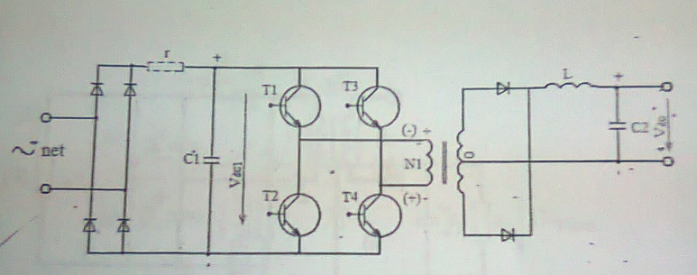
A power supply circuit utilizing frequent energy switching can be designed by first establishing a full-wave bridge rectifier configuration. This configuration employs four diodes arranged in a manner that converts alternating current (AC) input into direct current (DC). The output from this rectifier is often "bumpy," necessitating the incorporation of a smoothing capacitor (C1) to produce a more stable DC output. Additionally, a resistor (R) is included to limit the initial charging current to the capacitor, ensuring safe operation.
The primary operational component of the circuit is a transformer with a primary coil (N1). The transistors (T1, T2, T3, and T4) are arranged to control the flow of current through this coil. When T1 and T4 are activated, current flows from the top to the bottom of the coil, resulting in a positive voltage at the top and a negative voltage at the bottom. Conversely, when T2 and T3 are engaged, the voltage polarity reverses, allowing current to flow from the bottom to the top, thus generating alternating current (AC) through the primary coil.
A critical aspect of this design is the electronic control system, which is responsible for switching the transistors on and off in pairs. This system must be carefully designed to ensure that at no time are all transistors activated simultaneously, as this could lead to circuit failure and potential damage. The inclusion of an inductor is beneficial for mitigating voltage spikes that may arise from the rapid switching actions of the transistors.
To implement the control system, a square wave oscillator can be utilized, with a duty cycle set to 50%. A 555 timer configured in astable mode can generate the required square wave, followed by a frequency divider circuit, such as a JK or D-type flip-flop, to produce complementary outputs for controlling the bases of the transistors. The duty cycle can be adjusted to ensure that the switching frequency is appropriate for the application.
Furthermore, it is advisable to integrate snubber diodes across the transistors (between collector and emitter) to protect against back electromotive force (EMF) generated when the current in the primary coil is interrupted. This protection is essential to maintain the integrity of the transistors and enhance the reliability of the circuit.
Overall, while this description outlines a fundamental approach to designing a power supply circuit with energy switching capabilities, it remains theoretical. Further considerations regarding signal interfacing, timing, and feedback control would be necessary for a more robust and practical implementation.A power supply with frequent energy switching; but the schematic is incomplete. I should add another circuit which controls the voltage polarity converter (Four transistors). The circuit generates high frequency current pulses. @CamilStaps Actually I didn`t know what to do! Where to start! I have no idea about the "voltage polarity converter" and its controlling circuit. Sorry about any inconvenience, but I will appreciate any though would explain the thing. Siraj Muhammad May 16 `13 at 18:41 @SirajMuhammad What objectives do you have to reach in this homework (This is more like a practicum assignment since you have to physically build the device. ) Nick Alexeev™ May 16 `13 at 18:48 @pjc50 50 or 60Hz transformer would be much larger than a high-frequency transformer (say, 100kHz).
The circuit in the question has more moving parts, but it`s smaller and cheaper than having a low frequency transformer. Nick Alexeev™ May 16 `13 at 19:24 The starting point I would take with this circuit is to break the diagram down into functional blocks (or sub systems).
Reading the circuit from INPUT ->-OUTPUT (Left to Right as drawn) On the left hand side we have 4 DIODES arranged in a conventional (full wave) bridge rectifier configuration converting the AC input into (bumpy) DC. C1 is the smoothing capacitor that gets rid of the bumps (hopefully) and R is either a real or `implied` circuit resistance to limit the initial charging current to the capacitor.
The output across C1 is (or should be) smooth DC. ~ (charge time constant(Seconds) = R(ohms) x C(Farads) - so far this is a very standard circuit and requires no further changes. When T1 and T4 are turned ON a current will flow through the PRIMARY COIL (N1) so that the TOP connection is POSITIVE and the BOTTOM connection is NEGATIVE - i.
e. conventional current flow is TOP(+) to BOTTOM(-). When T2 and T3 are switched ON the BOTTOM of the coil becomes POSITIVE and the TOP connection becomes NEGATIVE. i. e. current flow is BOTTOM(+) to TOP(-) thus producing and Alternating Current (AC) through the primary coil by switch the direction of the DC.
What is MISSING from this block is the electronic control system to switch each pair of transistors ON and OFF ensuring that AT NO TIME are ALL the transistors turned on (nasty things will happen and the magic blue smoke that makes all electronic devices work will escape and never work again). This is a standard circuit for FULLWAVE rectification and smoothing from a centre tapped transformer.
It does not require any addition or modification. The inductor is very good for taking out spikes that will be generated by the switching action of the transistors. In the simplest case this would consist of a SQUAREWAVE oscillator (50% duty cycle) with COMPLIMENTARY outputs.
e. g a simple 555 astable followed by a `divide by 2` circuit such as a JK or D type flip flop. The 555 would run at TWICE the switching frequency. . The divider will set the duty cycle to 1:1 (ON to OFF) I would also add FOUR snubber diodes across the transistors (C-E) (diodes connected the `wrong` way to prevent transistor damage from back emf when the current though the primary inductor is turned OFF). From the `Q` output of the divider connect the bases of T1 and T4 through separate resistors. From the `NOT Q` output connect the bases of T2 and T3 via separate resistors. This is a very theoretical and simplistic circuit solution - No consideration is given to properly interfacing control signals, signal timing, type, feedback control etc.
The switching input is just a simple square wave. Switching the load ON is not a problem as the inductor will cause the current to rise slowly (L/R time constant). The problem happens when the transistor is turned OFF - the inductor`s magnetic field collapses and induces a very high (E proportional to dB/dT) voltage in the reverse d
🔗 External reference
Related Circuits
A 175 MHz high-frequency amplifier circuit utilizing a field-effect transistor (FET) is presented. The field-effect transistor used is the 3D04H, along with its associated components and parameters. The 175 MHz high-frequency amplifier circuit is designed to amplify signals in the...
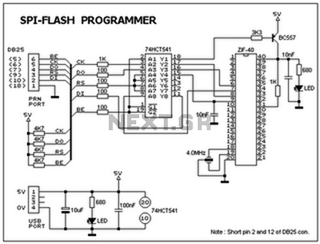
This ISP programmer can be utilized for both in-system programming and as a standalone SPI programmer for Atmel ISP programmable devices. The programming interface is compatible with the STK200 ISP programmer hardware, allowing users of STK200 to employ the...
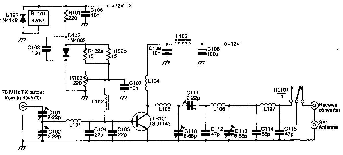
This 70 MHz RF power amplifier circuit utilizes the SD1143 transistor, which offers a gain of approximately 14 dB in this configuration. The design leverages the characteristics of a 175 MHz device. The RF power amplifier circuit designed around the...
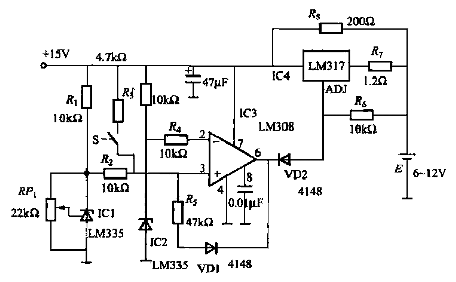
When fast charging a nickel-cadmium battery, the temperature control circuit, as illustrated in the accompanying figure, is designed to monitor the battery temperature to regulate the charging current. The circuit consists of Icl to IC3, which forms the temperature...
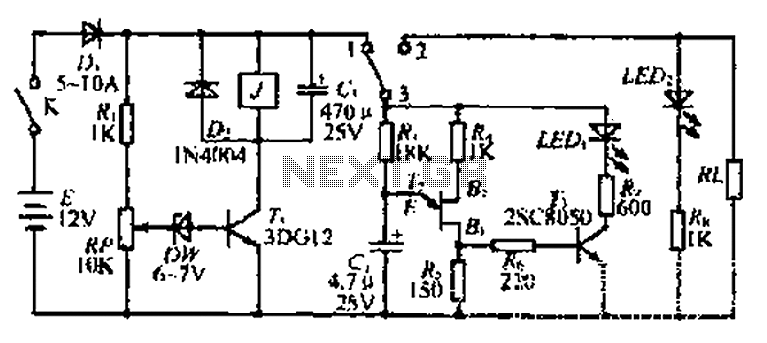
The discharge control circuit consists of a battery management system designed to prevent over-discharge of a battery. It features a relay control mechanism that activates when the battery voltage drops below a specified threshold of approximately 10.5V. The circuit...
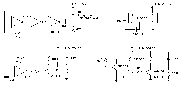
The LED flasher circuits below operate on a single 1.5 volt battery. The circuit on the upper right uses the popular LM3909 LED flasher IC and requires only a timing capacitor and LED. The top left circuit, designed by...
Warning: include(partials/cookie-banner.php): Failed to open stream: Permission denied in /var/www/html/nextgr/view-circuit.php on line 713
Warning: include(): Failed opening 'partials/cookie-banner.php' for inclusion (include_path='.:/usr/share/php') in /var/www/html/nextgr/view-circuit.php on line 713