
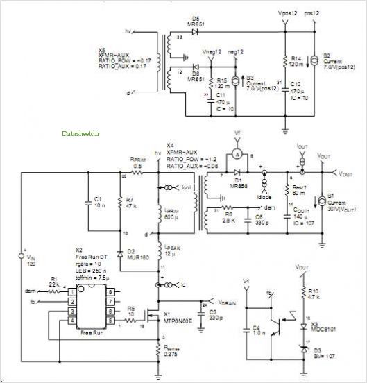
power supply NMOS FET selection for reverse polarity protection
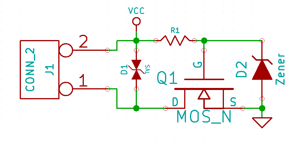
The reverse polarity protection circuit is designed to safeguard sensitive electronic components from damage caused by incorrect power supply connections. In this specific design, the circuit must accommodate a broad input voltage range of 5-40V, which presents challenges in selecting appropriate MOSFETs. The gate-source voltage (VGS) limitation of common MOSFETs, typically capped at 20V, necessitates the implementation of a Zener diode clamp to restrict the gate voltage within safe operational limits. This ensures that the MOSFET can be driven adequately without exceeding its maximum ratings.
The maximum anticipated input current of 6A necessitates careful consideration of the FET's characteristics. The drain-source breakdown voltage (BVDSS) must be selected to exceed the maximum input voltage to prevent breakdown during reverse polarity conditions. Additionally, minimizing the on-resistance (RDS(on)) is essential to maintain efficiency and reduce heating in the circuit, especially in high-current applications.
The operational characteristics of the MOSFET in the Ohmic region are critical to the circuit's performance. When the drain-to-source voltage (VDS) is minimal, the drain current (ID) is also expected to be low, which can reduce power dissipation. However, in environments with potential electrical noise, such as those with motors, voltage offsets between different grounds can introduce complications. These offsets may inadvertently allow current to flow even when the intended state is off.
To mitigate these risks, the design can incorporate a Zener diode to clamp VGS closer to the threshold voltage (VGS(th)). This approach helps to limit the drain current and voltage under various operational conditions, thereby enhancing the reliability and safety of the reverse polarity protection circuit. Overall, careful selection of components and thoughtful circuit design are paramount to achieving effective reverse polarity protection in this application.A reverse polarity protection circuit, similar to that in Figure 2 of SLVA139: Reverse Current/Battery Protection Circuits. Here is my circuit: My case is slightly more complex due to the possible input voltage ranging from 5-40V.
Most MOSFETs seem to have a maximum gate-source voltage VGS of 20V, so I need the Zener clamp on thegate (or a very large/expensive FET). The maximum input current will be about 6A. What I`m wondering is, what FET characteristics actually matter in this configuration I know that I definitely want a drain-source breakdown voltage BVDSS high enough to handle the full input voltage in the reverse polarity condition. I`m also pretty sure I want to minimize RDS(on) as to not introduce any impedance in the ground circuit.
Fairchild AN-9010: MOSFET Basics has this to say about operation in the Ohmic region: "If the drain-to-source voltage is zero, the drain current also becomes zero regardless of gate to-source voltage. This region is at the left side of the VGS VGS(th)= VDS boundary line (VGS VGS(th) > VDS > 0). Even if the drain current is very large, in this region the power dissipation is maintained by minimizing VDS(on).
" Does this configuration fall under the VDS = 0 classification That seems like a somewhat dangerous assumption to make in a noisy environment (this will be operating in the vicinity of various types of motors), as any voltage offsets between input supply ground and local ground could cause current to flow. Even with that possibility, I`m not sure I need to spec for my maximum load current on the drain current ID.
It would then follow that I don`t need to dissipate very much power either. I suppose I could mitigate the problem by Zener clamping VGS closer to VGS(th) to reduce drain current/voltage 🔗 External reference
Related Circuits
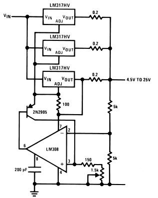
The LM317HV adjustable regulator is capable of supplying over 1.5A across an output voltage range of 1.2V to 57V. The design of this high current power supply is straightforward, as the LM317HV requires only a few external resistors to...
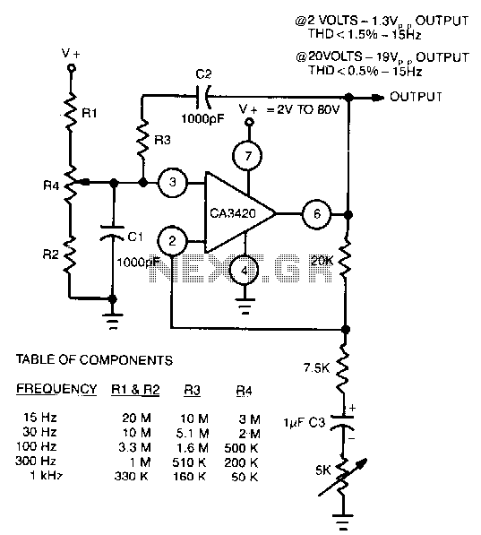
The adjustment of R4 contributes to the comparatively symmetrical output transfer characteristic of the CA3420 BiMOS operational amplifier. To extend the lower operating frequency, remove C3 and use a dual supply. The CA3420 is a high-performance BiMOS operational amplifier that...
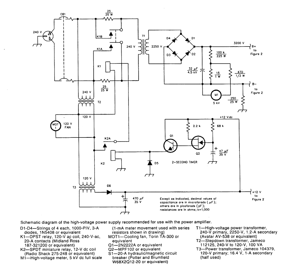
A schematic diagram of the high-voltage power supply recommended for use with the power transformer. This power supply can also be used for other equipment with similar requirements. CAUTION: hazardous high voltages. The high-voltage power supply schematic is designed to...
This application note demonstrates a simple 8-direction digital compass application utilizing Zilog's Z8 Encore!® MCU and an external compass sensor hardware. Communication ports are provided for the digital compass to receive commands and send status via the I2C bus...
To celebrate the hundredth design posted to this website and to fulfill the requests of many correspondents wanting an amplifier more powerful than the 25W MosFet, a 60 - 90W high-quality power amplifier design is presented here. The circuit...
A Common Cathode LED strip is being utilized instead of a Common Anode variant, leading to the development of a modified circuit. The experience with FETs was limited, resulting in challenges as a minimum voltage equal to Vcc is...