
Practical Circuit Design Technique in Boosting Current Limit of CLDs by Using Transistor Current Gai
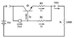
The practical current booster circuit technique is a method used to enhance the current capacity of a circuit beyond the limitations of standard components. The conventional circuit design typically employs a Constant Current Load (CLD) configuration, which stabilizes the output current despite variations in load or supply voltage. This technique is particularly useful in applications where high current is required but the available components cannot handle such loads directly.
The analysis of the booster circuit principle focuses on the operational characteristics of the circuit, including its input-output relationships, efficiency, and stability under varying conditions. It is essential to understand the fundamental principles governing the operation of the circuit to optimize its performance and ensure reliability.
Implementation considerations for the circuit include selecting appropriate components, such as the NPN CZT3055 and PNP CZT2955 transistors, which are known for their high current handling capabilities. Proper thermal management must also be addressed, as high current operation can lead to significant heat generation. Adequate heat sinks and thermal interfaces are necessary to maintain the transistors within safe operating temperatures.
The exemplary experimental results provided in the datasheet illustrate the effectiveness of the current booster circuit technique. Graphs and charts may depict the performance metrics, showcasing how the circuit meets or exceeds design expectations. The illustrations serve to clarify the circuit layout and operation, providing valuable insights for engineers looking to implement similar designs in their applications.
Overall, this application datasheet serves as a comprehensive resource for engineers seeking to understand and apply current booster circuit techniques in their projects.What you will find in this aplication datasheet article are sections that discuss about the practical current booster circuit technique (conventional circuit using CLD, current boosting circuit technique), the analysis of booster circuit principle, the implementation of circuit considerations, and an exemplary experimental result with ilustration using NPN CZT3055/ PNPCZT2955 transistors 🔗 External reference
Related Circuits
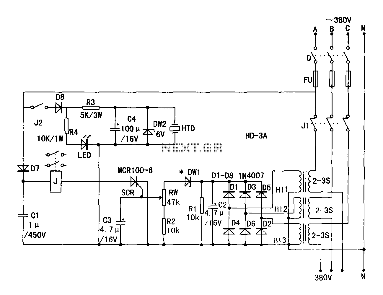
A current transformer H11-3 needs to be constructed. Select a transformer core with a minimum power rating of 2W for the first secondary winding. Use enameled wire with a diameter of 0.12 mm and wind approximately 1000 turns. The...
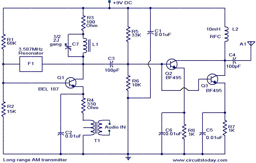
The circuit diagram of an AM transmitter circuit based on three transistors. With correct tuning and a matching antenna, the transmitter can effectively transmit amplitude-modulated signals. The AM transmitter circuit utilizes three transistors configured to amplify and modulate the input...
Electron trajectories in a conductor are depicted in the diagrams below. When no electric field is present inside a conducting material, electrons move randomly. However, when an electric field is applied, the electric force F = qE induces a...
The LM380 is a power audio amplifier designed for consumer applications. To minimize system costs, the gain is internally fixed at 34 dB. It features a unique input stage that allows for ground-referenced input signals. The output automatically self-centers...
The 10A H-Bridge Motor Controller circuit appears straightforward, but several critical aspects should not be overlooked. The primary components utilized in the circuit include the TIP147, TIP142, and 2N2222 transistors. The power supply circuit operates at +12V, which is...
A low-cost vacuum cleaner system based on the P89LPC901 is introduced in this application note. The design hardware and software are thoroughly discussed. This system can also guide the design of other universal motor driving systems that require robust...