
Practical Transistor Circuits

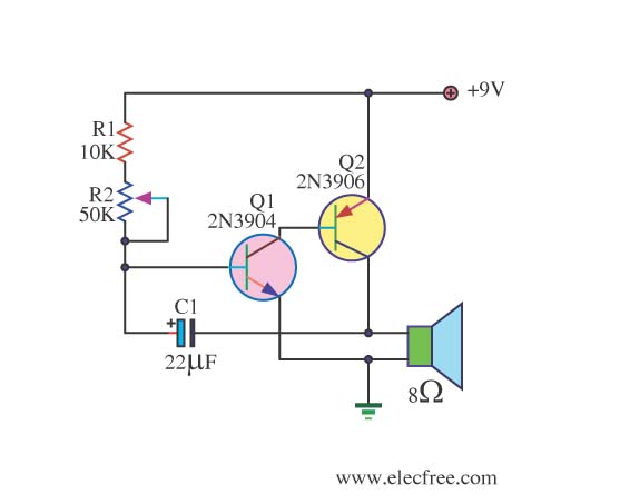
A schematic for a general-purpose, low-power, high-gain amplifier using discrete transistors is provided. This Class-A amplifier can drive loads such as speakers or headsets with impedances greater than 65 ohms, drawing a quiescent current of approximately 20 milliamperes, which can be reduced by increasing the value of resistor R3. Transistors Q1 and Q2 are arranged as common-emitter amplifiers, with the output of Q1 directly coupled to the input of Q2, resulting in an overall voltage gain of about 80 dB. Resistor R3, which serves as the emitter load for Q2, is decoupled by capacitor C3, allowing the emitter of Q2 to follow the average collector voltage of Q1. The base bias for Q1 is obtained from Q2's emitter via R2, providing stabilization through negative DC feedback. An input potentiometer, R4, acts as the volume control for the circuit.
Additionally, a schematic for a simple three-transistor Class-AB complementary amplifier is included, which can deliver around 1 watt into a 3-ohm speaker load. In this configuration, Q1 operates as a common-emitter amplifier, driving a load that includes speaker SPKR1, resistor R1, and potentiometer R5. The output voltage is subsequently followed and amplified by the complementary emitter-follower stage comprising Q2 and Q3. The output is transmitted through capacitor C2 to the junction of SPKR1 and R1, providing a low-impedance drive for SPKR1 while simultaneously bootstrapping R1 to achieve high voltage gain. Feedback from the output to the base of Q1 through R4 forms a negative feedback loop for biasing. The trimmer potentiometer R5 should be carefully adjusted to minimize audible crossover distortion while maintaining the lowest measurable quiescent current, ideally set between 10 to 15 milliamperes.
Furthermore, a more complex audio power amplifier capable of delivering approximately 10 watts into an 8-ohm load when powered by a 30-volt supply is described. This circuit consists of four high-gain, quasi-complementary output stages (Q3 to Q6), with Q1 serving as an adjustable amplifier diode output biasing device. The main load resistor R2 in the Q2 common-emitter amplifier stage is bootstrapped by capacitor C2 and DC biased by resistor R3, which should be adjusted to set the quiescent output voltage at about half the power supply voltage. If this is not achieved, the value of R3 should be altered. The upper frequency response of the amplifier is limited by capacitor C3, which may compromise circuit stability. Additionally, capacitor C5 is connected in series with R8 across the amplifier's output to enhance stability. The amplifier should initially be set up following the guidelines provided for the circuit in Figure 2.
Despite the decline in popularity of records (LPs) with the advent of compact discs (CDs/DVDs), manufacturers have recently reintroduced record players, catering to the enduring interest in vinyl records.This last article on bipolar junction transistors (BJT) is a potpourri of circuits. Some are practical and some are not so practical, but they can be great for experiments. With these circuits you can amplify signals, filter high and low frequencies, generate white noise, and flash lamps. You can also boost DC voltage levels, locate hidden metal o bjects, and detect rising water. One circuit will even demonstrate the fundamentals of lie detection! Today the easiest way to build a low- to medium-power audio amplifier is to pick an integrated circuit (IC) amplifier from a manufacturer`s data book and supplement it with additional components recommended in the applications notes in the data book. However, if you just want to learn amplifier principles by experimentation or you have a simple application in mind, you should build the amplifier with discrete transistors.
Figure 1 is a schematic for a general-purpose, low-power, high-gain amplifier based on discrete transistors. A Class-A amplifier, it can drive a load such as a speaker or headset with an impedance greater than 65 ohms.
The amplifier draws a quiescent current of about 20 milliamperes. However, this drain can be reduced by increasing the value of R3. Transistors Q1 and Q2 are configured as common-emitter amplifiers; the output of Q1 is directly coupled to the input of Q2. This circuit has an overall voltage gain of about 80 dB. Notice that resistor R3, the emitter load of Q2, is decoupled by capacitor C3 so that the Q2 emitter follows the average collector voltage of Q1.
The base bias for Q1 is derived from Q2`s emitter through R2. With this configuration, the bias is stabilized by negative DC feedback. Input potentiometer R4 serves as the circuit`s volume control. Figure 2 is the schematic for a simple, three-transistor, Class-AB complementary amplifier which can drive about 1 Watt into a 3-ohm speaker load. Transistor Q1, which is configured as a common-emitter amplifier, drives a load that is the sum of speaker SPKR1.
resistor R1 and potentiometer R5. Its output voltage is followed and boosted in power by the complementary emitter-follower stage made up of Q2 and Q3. The output of the amplifier is fed through capacitor C2 to the junction of SPKR1 and R1 where it provides a low-impedance drive for SPKR1.
It simultaneously bootstraps the value of R1 so that the circuit has high-voltage gain. The output is also fed back to Q1`s base through R4 so that it produces a base bias through a negative feedback loop. Carefully adjust trimmer potentiometer R5 to minimize audible signal crossover distortion so that it is consistent with lowest quiescent current consumption that can be measured.
To obtain a reasonable value, set the quiescent current from 10 to 15 milliamperes. Figure 3 shows a more complex audio power amplifier that can deliver about 10 watts into a 8-ohm load when powered from a 30-volt supply. This circuit includes four, high-gain, quasi-complementary output stage (Q3 to Q6). Transistor Q1 functions as an adjustable amplifier diode output biasing device in this circuit. The main load resistor R2 of the Q2 common-emitter amplifier stage is bootstrapped by C2 and DC biased by R3.
This network should set the quiescent output voltage at about half the power supply value. If it does not, alter the value of R3. The upper frequency response of the amplifier is restricted by C3, which menaces circuit stability. In addition, capacitor C5 is wired in series with R8 across the output of the amplifier to increase circuit stability. The amplifier should be set up initially as was described for the circuit in Fig. 2. Today, with the widespread acceptance of compact discs (CDs/DVDs), records (LP) are long obsolete. However, because of the everlasting popularity of the record (it seems), the last couple years manufacturers have been bringing back the old record player in a new coat.
Like myself, many people still 🔗 External reference
Related Circuits
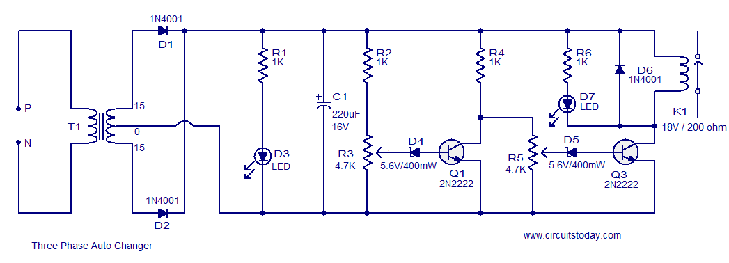
The following circuit illustrates a Three Phase Auto Changer Circuit Diagram. This circuit utilizes the 2N2222 transistor. Features include a transformer. The Three Phase Auto Changer Circuit is designed to automatically switch between different phases in a three-phase power system,...
The circuit employs two Light Dependent Resistors (LDRs) arranged in series with a separation of approximately half a meter. This configuration allows each LDR to detect the presence of a person entering or exiting the room. The processed outputs...
The 786A multi-functional double-tube fluorescent emergency circuit is illustrated in Figure 2-129. This circuit shares similarities with Figure 2-125. The 786A multi-functional double-tube fluorescent emergency circuit is designed to provide illumination during power outages or emergencies. It utilizes two fluorescent...
This circuit is a simple metronome model designed for ease of use. It employs transistors as key components, specifically configured as an astable multivibrator, to produce a beeping sound. The tone can be adjusted using a variable resistor (VR1)....
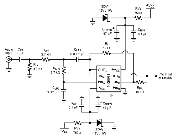
The ICs LM4651 and LM4652 are types of MOSFET integrated circuits and power amplifiers that include high-efficiency amplifiers, making them suitable for self-powered speakers, subwoofers, and high-quality car audio systems. The LM4651 is a fully integrated conventional pulse width...
Electronic temperature control circuit for imported car air conditioners. It utilizes operational amplifiers A1 and A2, specifically the LM393 model. An adjustment potentiometer (RP) is included, allowing modification of the temperature range. The adjustment range includes a power temperature...