
Preamplifier and Bandpass filter for SDR
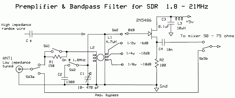
The SDR hardware described is engineered to provide a flexible and high-performance platform for radio frequency applications. Its architecture allows for effective manipulation of signal processing through the use of a balanced mixer and low noise amplification. The design considerations emphasize the importance of impedance matching and minimizing distortion, especially in environments with varying signal conditions. The inclusion of a variable capacitor and high-Q inductors ensures that the system can adapt to a wide range of frequencies, while the step attenuator allows for precise control over gain, enhancing usability in diverse operational scenarios.
The circuit's performance can be further optimized by careful selection of components, particularly in the choice of inductors and capacitors, which directly influence the Q-factor and overall sensitivity. The use of a toroidal core for inductors is a strategic decision that maximizes coupling efficiency and minimizes losses. Furthermore, the design allows for easy modifications, enabling users to tailor the SDR to specific applications or frequency ranges, thus enhancing its versatility.
In practical applications, this SDR setup is suitable for a variety of tasks, including amateur radio, signal intelligence, and experimental communications. Its ability to maintain performance across a broad frequency range while addressing potential issues such as harmonic mixing and second-order distortion makes it a valuable tool for both hobbyists and professionals in the field of electronics and telecommunications.The SDR hardware in its simplest form consists of a wideband switched balanced mixer and low noise LF amplifier. This simple hardware has an amazing sensitivity and linearity which is sufficient for test and even regular use.
Here are some of the problems in this simple hardware: 1. The mixer is converting also the input spectrum around odd harmon ics of the oscillator. For example the theoretical attenuation of the third harmonic mixing versus first harmonic is only 10 dB. 2. The sensitivity of this simple SDR is somewhere around -124dBm to -128 dBm at 500 Hz bandwidth (with good low noise preamplifier).
But sometimes there are conditions, on higher frequencies, when the atmospheric noise is very low and the sensitivity should be above -130dBm. 3. The second order distortions are the weak point of this type of radio. To avoid these effects, an input filter is needed for out of band strong stations and also a step attenuator.
4. The switched mixer has excellent parameters when the signal source has low and resistive internal resistance. The antenna as a signal source is not the best choice even if the antenna is tuned, not to mention the random wires.
The image rejection and dynamic range are drastically reduced when the signal source has reactive component. 5. There is strong leakage signal of the heterodyne oscillator at the mixer input. This signal is heard as a strong carrier if a second receiver uses the same antenna. A parallel L1, C1 circuit with high Q-factor is tuned with variable capacitor in the range from 1. 8 to 18 MHz. The signal from the low Z antenna is fed with inductive coupling with transformation ratio 1:12. The FET follower transforms the high resonance impedance into low resistive impedance which is fed to the switch mixer.
The voltage gain actually takes place by the 1:12 transformation. The gain can be reduced in 6 dB steps by switching the FET gate to different taps of the inductive coil. The taps are ½, . and 1/8 of windings referred to ground. There is additional attenuator with single resistor R1. When R1 is inserted, the Q-factor of the LC circuit increases due to reduced load from the antenna side.
The variable capacitor is a plastic type from MW receiver. The two sections (5 - 235 pF) are connected in parallel. The inductance L1 is wound on toroidal ferrite core from HF low loss material (mu = 80). Iron powder high Q cores might be used also. The inductance must be 4. 7 uH which in our case is reached with 12 turns. The measured Q factor at 10 MHz was 200. L2 has only 1 turn on the same core. It is good for a L1 and L2 to be wound on toroidal core since the magnetic coupling between two windings will be strong. I have tested a very lazy solution with a commercial 4. 7 uH choke. The Q-factor at 10 MHz was 90 and L2 has 2 turns wounded tightly above color markings of the choke. The results are quite satisfactory but the possibility of gain switching is missed. Nothing in this design is critical. Keep the 4. 7 uH value of L1 if the entire range 1. 8 -20 MHz is needed. For 1. 8 MHz band additional capacitor of 1300 pF is added. The drain current is 9 mA but will depend from the type of the transistor used and the range might be 5 15 mA.
This simple circuit was simulated with CAD simulator LTspice. This is a freeware simulator from Linear Technology. For those who are interested I am giving the working file RF_preamp. asc. The results are presented on Table 1. The first column is the voltage gain. The second is the effective Q-factor which determines the selectivity and the third column is the attenuation for 3 times higher frequency. Two cases with R1 on and short circuited are presented. The unloaded Q-factor of L1 was defined 200 on all bands. The frequency responses for 7 MHztune frequency are presented on Fig. 3. The frequency response is not changed by the gain switching. There is some shift in resonance frequency when the taps are s 🔗 External reference
Related Circuits
The graphs below illustrate the computer predictions of filter performance provided by Harry PA0LQ. Click on the thumbnail to view the full-size graph. A significant challenge in aligning the filter was the lack of access to a frequency counter...
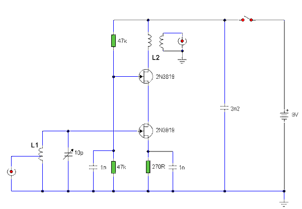
The lower FET operates in common source mode, while the upper FET operates in common gate mode, achieving full high-frequency gain. The bottom FET is tunable, allowing for peak adjustment for a particular station. Coil details follow: The described circuit...
%2B2%2BCH%2Bby%2BIC%2B%2BNE5532%2Bor%2BLF353.jpg)
This is a microphone preamplifier circuit model 2 CH. The circuit utilizes integrated circuits NE5532 or LF353 to amplify the sound signal from a dynamic microphone, increasing the power level for subsequent input into a stereo power amplifier. This...
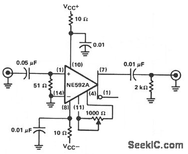
The circuit provides a voltage gain of 20 ±0.1 dB within a frequency range of 500 kHz to 50 MHz. The low-frequency response of the amplifier can be enhanced by increasing the value of the 0.05 µF capacitor connected...
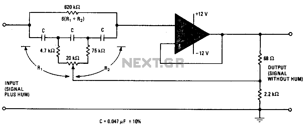
This narrow stop-band filter can be adjusted using a potentiometer to position the notch frequency anywhere from 45 to 90 Hz. It effectively attenuates power-line hum and other unwanted signals by at least 30 dB. The circuit is cost-effective...
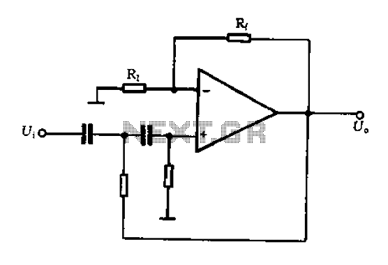
A typical two high-pass filter circuit. A high-pass filter (HPF) is an electronic circuit that allows signals with a frequency higher than a certain cutoff frequency to pass through while attenuating signals with frequencies lower than the cutoff frequency. A...
Warning: include(partials/cookie-banner.php): Failed to open stream: Permission denied in /var/www/html/nextgr/view-circuit.php on line 713
Warning: include(): Failed opening 'partials/cookie-banner.php' for inclusion (include_path='.:/usr/share/php') in /var/www/html/nextgr/view-circuit.php on line 713