
Precision-Increasing Buffer
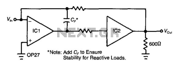
In an analog circuit, the integration of a unity-gain buffer is a strategic enhancement that significantly improves signal integrity and precision. The operational amplifier IC1, characterized by its maximum offset voltage drift of 1.8 µV/°C, is capable of driving a load of 600 ohms. The power dissipation of IC1 under these load conditions is calculated to be 94 mW, which is critical for thermal management in circuit design. The thermal resistance (θJA) of 150°C/W indicates that for every watt of power dissipated, the junction temperature will rise by 150°C. This results in a change in output voltage of 25 µV, which could adversely affect the precision of the circuit.
By incorporating a unity-gain buffer IC2, the design effectively isolates IC1 from the load, thus preventing variations in power dissipation from affecting the operational characteristics of IC1. This isolation is crucial for maintaining the minimum rated offset voltage, ensuring that the output remains stable and accurate. The loop gain of IC1 plays a vital role in this configuration, as it serves to cancel out any potential offset introduced by the buffer, thereby preserving the integrity of the signal.
When selecting a suitable unity-gain buffer, it is essential to consider its bandwidth characteristics. A buffer with a 3-dB bandwidth at least five times greater than the gain-bandwidth product of the operational amplifier will ensure that the buffer operates effectively within the desired frequency range without introducing significant phase shifts or distortion. This consideration is paramount for applications requiring high precision and reliability in analog signal processing. Adding an unity-gain buffer to your analog circuit can increase its precision. For example, by itself, the op a mp IC1 exhibits a maximum dVosldT of 1.8 /iV7°C and can drive a 600- load. Under these conditions, IC1 would dissipate 94 mW incrementally. Thus, the op amp"s 0JA of 150°C/PFr would change its vqs by 25 juY. The buffer, IC2, will isolate IC1 from the load and eliminate the change in power dissipation in IC1, thereby achieving ICl"s minimum, rated offset-voltage drive. The loop gain of IC1 essentially eliminates the offset of the buffer. Almost any unity-gain buffer will work, provided that it exhibits a 3-dB bandwidth that is at least 5 times the gain-bandwidth product of the op amp.
🔗 External reference
Related Circuits
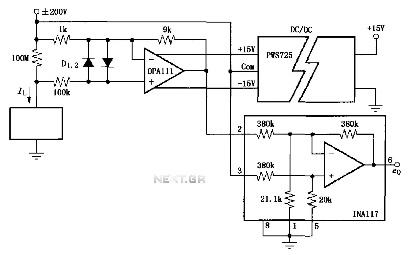
The circuit illustrated in FIG OPA111 is designed for measuring input buffer leakage current. The transistors D1 and D2, which are 2N3904 types, short the base and collector contacts while leaving the emitter open. When a power supply of...
Cypress' Dave Van Ess cautions circuit designers about the excessive and careless use of operational amplifiers, providing examples and circuit theory. Operational amplifiers (op-amps) are widely utilized in various electronic circuits due to their versatility and performance characteristics. However, the...
The ZKJ-S-type buffer controller circuit is designed for motor starting slip control. This buffer controller is composed of two operational amplifiers, Ai and Az. The operational amplifier Ai functions as a speed amplifier that saturates, while Az acts as...
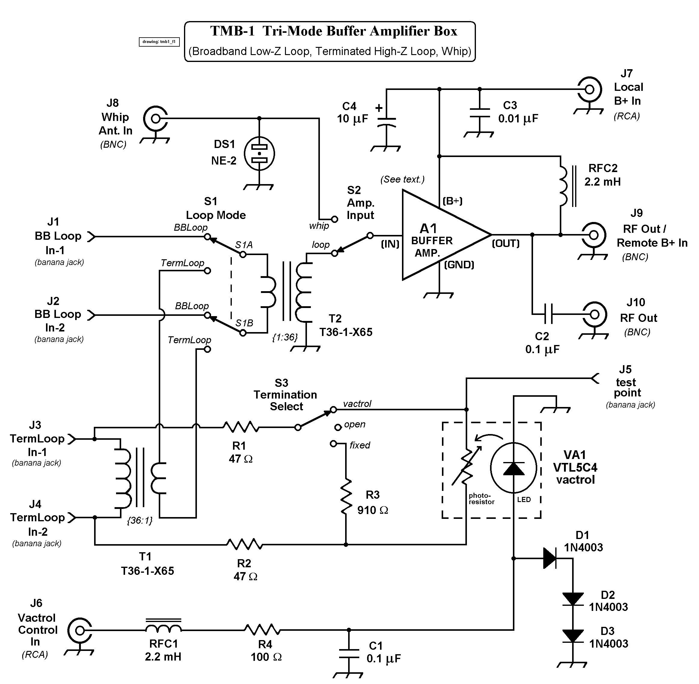
The TMB-1 is an RF amplifier unit and receiving accessory compatible with low-impedance broadband loops, high-impedance terminated loops (such as Pennant, Flag, or Kaz Delta), and whip (telescoping rod) antennas. This design is optimized for operation within the frequency...
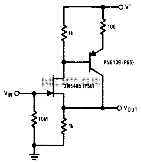
The 2N5485 features low input capacitance, making this compound series-feedback buffer a wide-band unity gain amplifier. The 2N5485 is a field-effect transistor (FET) that is often utilized in applications requiring low noise and high input impedance. Its low input capacitance...
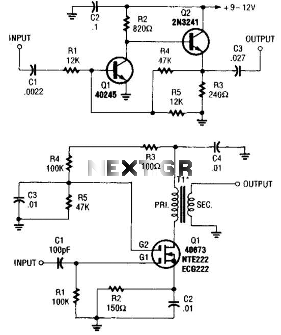
These two buffer/amplifiers have been effectively utilized with variable frequency oscillators (VFOs): one (depicted in A) is constructed using a pair of bipolar NPN transistors, while the other (illustrated in B) is designed around a dual-gate MOSFET. The first buffer/amplifier,...