
Buffer leakage current measurement circuit diagram OPA111 INA117
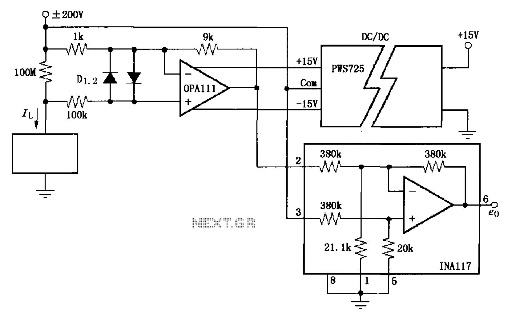
The OPA111 circuit configuration serves as a precise tool for measuring low-level leakage currents in high-voltage applications. The transistors D1 and D2, both configured as a Darlington pair, help maintain a high input impedance while ensuring minimal leakage current into the measurement path. This configuration is critical for applications where even minute currents can significantly affect the performance of sensitive electronic devices.
The 100MΩ sampling resistor is a key component in this setup, as it converts the leakage current into a measurable voltage drop. The INA117 instrumentation amplifier is selected for its high input impedance and low offset voltage, which are essential for accurate readings of small voltage changes that correspond to the leakage current. The output voltage from the INA117 is scaled to provide a clear and interpretable output, allowing for straightforward analysis.
The use of an isolated power supply for the OPA111 operational amplifier is particularly advantageous in this design. It ensures that the high voltage applied to the device under test does not affect the integrity of the measurement circuit. The ability to handle a common-mode voltage of up to 200V means that this circuit can be used in various high-voltage applications without the risk of damage or inaccurate readings.
Overall, this circuit design is an effective solution for accurately measuring leakage currents in high-voltage environments, leveraging high-impedance components and careful circuit design to ensure precision and reliability. As shown in FIG OPA111 constituted by the input buffer leakage current measuring circuit. D1, D2 of the transistor 2N3904, which will short the base and collector contact (open emitter). Up to 200V power is applied to the device under test, leakage current flows through 100M sampling resistor, forming a voltage drop across the sampling resistor, the voltage drop after the buffer input to the INA117 amplifier output, the output voltage eo IL 109 (1V/nA). Because you want to measure low leakage current, measurement circuit to prevent shunt caused by measurement error, so the use of high input resistance measurements constitute a buffer circuit.
With an isolated power supply OPA111 op amp power supply, so the circuit allows 200V common-mode range.
Related Circuits
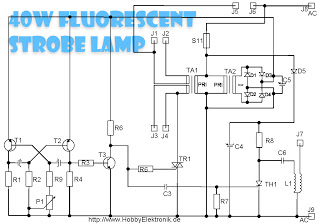
This circuit is designed for a 40 Watt fluorescent lamp. It operates similarly to a traditional strobe light, but utilizes a fluorescent tube instead. The fluorescent tube remains continuously energized, with both electrodes supplied with electricity. This current causes...
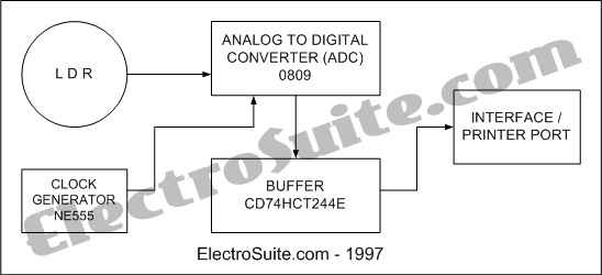
This is an illumination intensity measurement system diagram. The data in the microprocessor is always in digital form. This is an illumination intensity measurement system diagram - Part 1. The data in the microprocessor is always in digital form. The...

This is a circuit design for a digital voltmeter with an LED display. It is suitable for measuring the output voltage of a DC power supply. The circuit features a 3.5-digit LED display with a negative voltage indicator and...
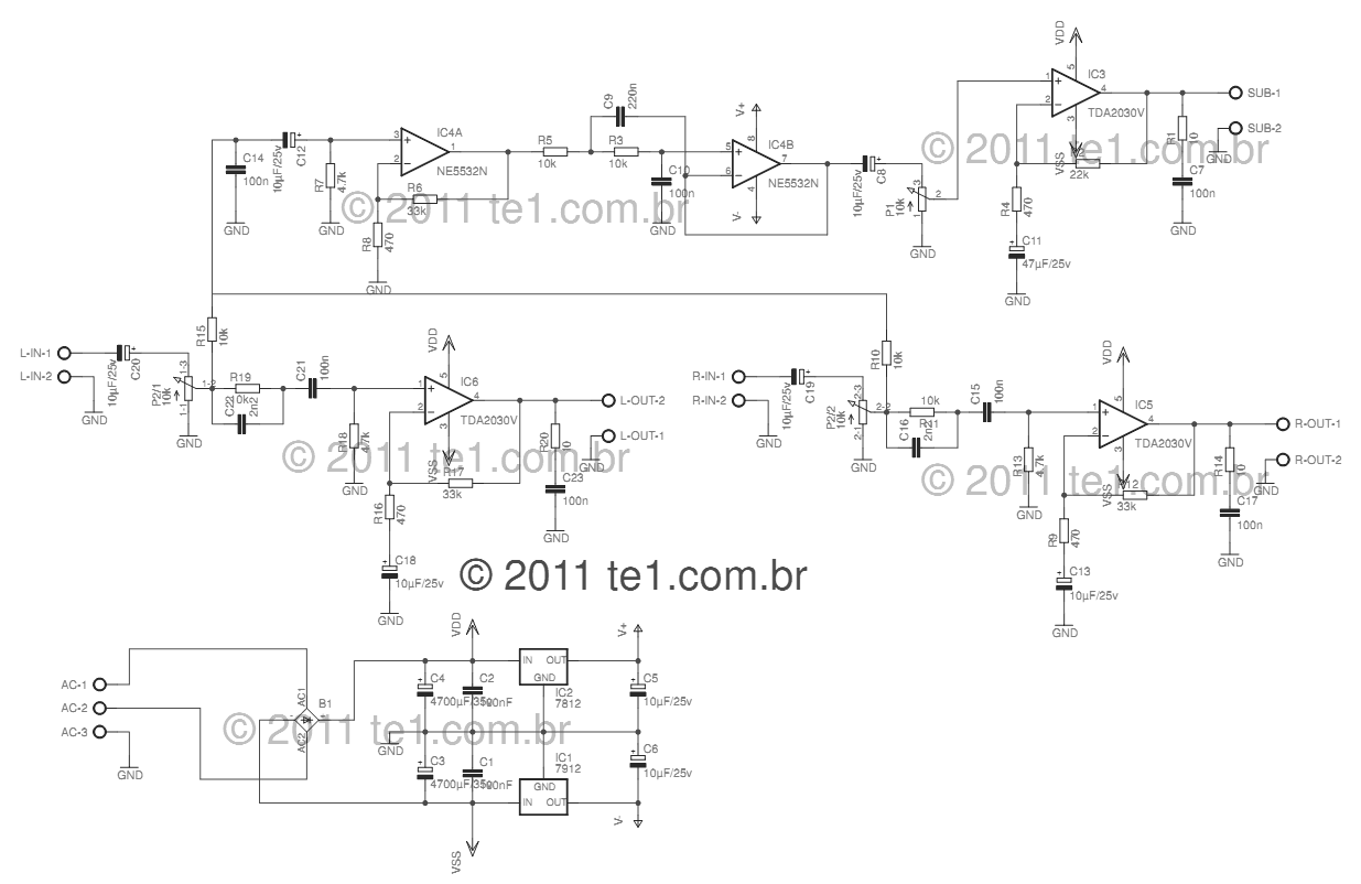
This circuit is a complete application for a 2.1 amplifier system, consisting of two satellite speakers powered by a TDA2030 and one subwoofer. This 2.1 system is commonly utilized in commercial applications as an amplifier for computers, enhancing audio...
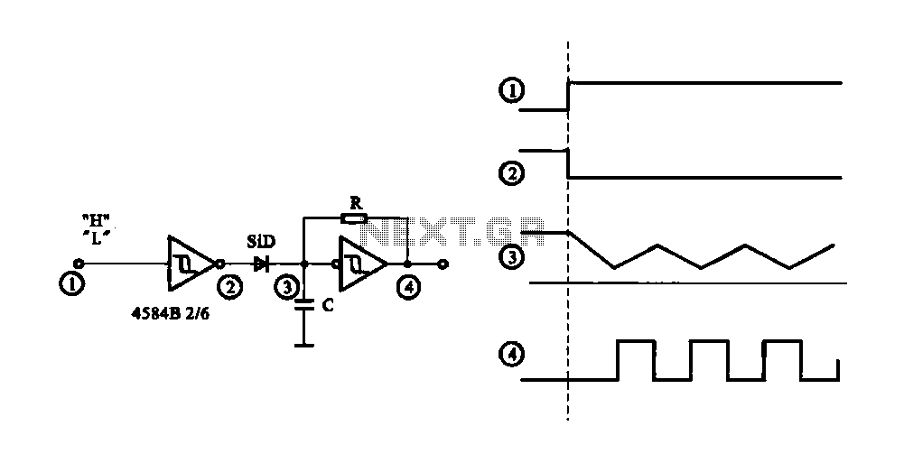
The circuit generates a controlled pulse signal. When a high pulse signal is applied to the input terminal O (start), the output pulse signal is activated. Conversely, when a low signal is received at the input terminal O (stop),...
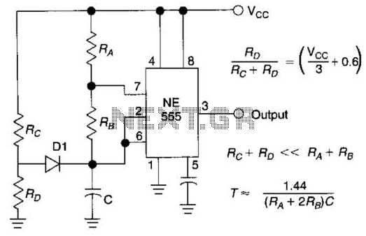
Using Rl, R7, and D1 to preset CI to one third of the supply voltage. This circuit avoids a longer first cycle period than subsequent cycles. The circuit described involves the use of resistors Rl and R7 along with diode...