
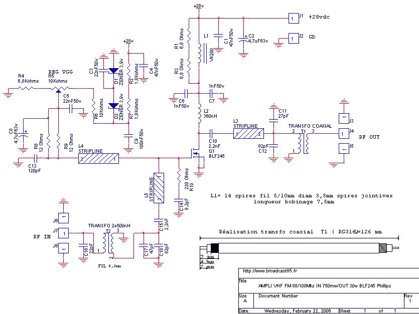
TMB-1 Tri-Mode Buffer Amplifier Box
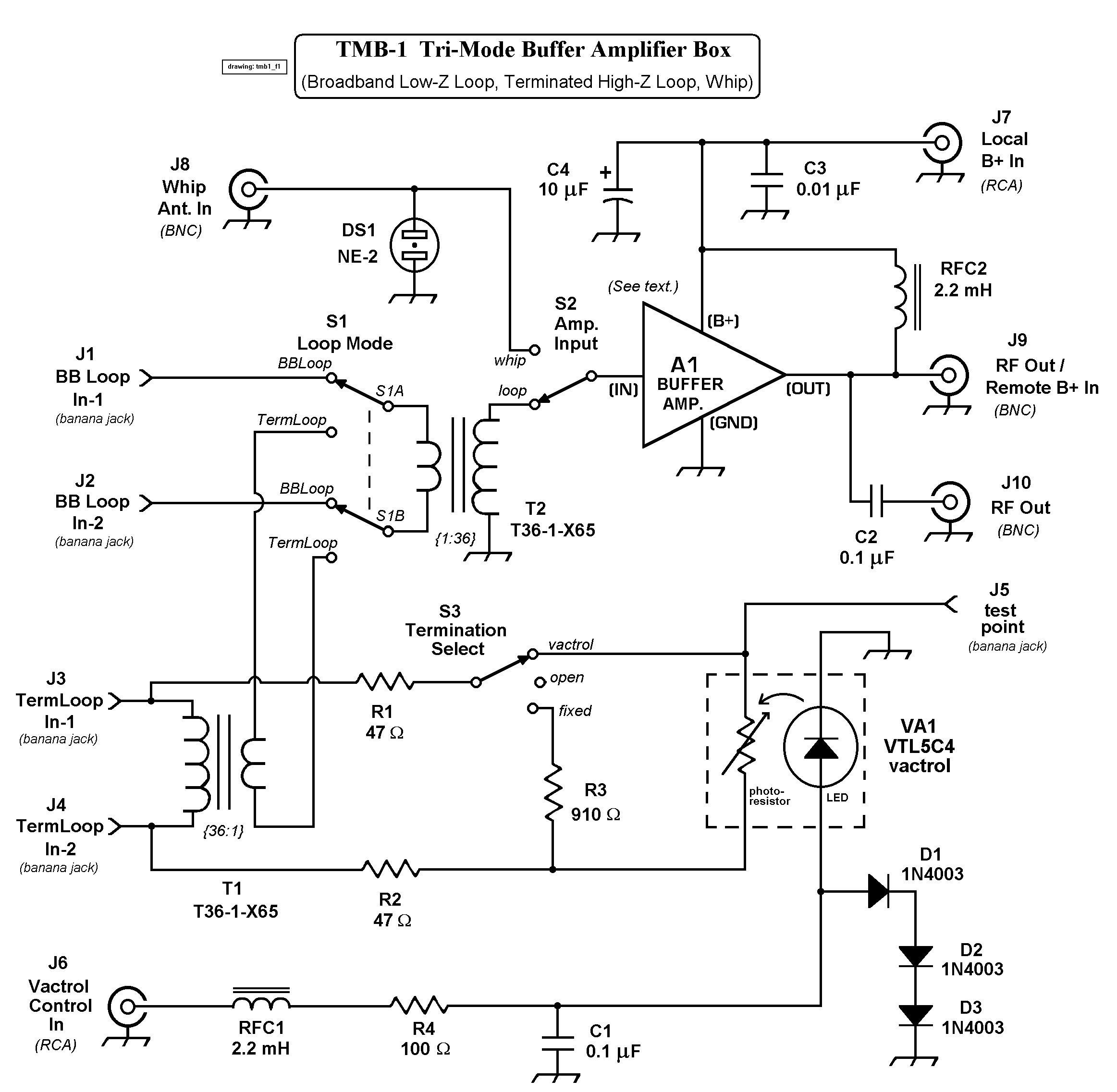
The TMB-1 circuit design incorporates various components that ensure effective amplification and signal processing. The RF transformers are critical in determining the frequency response and overall performance of the amplifier. The buffer amplifier is designed to maintain signal integrity while providing necessary gain, making it suitable for various antenna configurations. The inclusion of a bias tee allows for seamless integration of DC power and RF signals, facilitating flexible deployment of the antenna system. Furthermore, the TMB-1's adaptability to different antenna types enhances its utility in diverse operational scenarios, making it a versatile tool for radio frequency applications. The performance metrics achieved during testing indicate that the TMB-1 can effectively amplify weak signals, making it a valuable asset for amateur radio enthusiasts and professionals alike. The design considerations and testing results underscore the importance of optimizing the amplifier for specific frequency ranges to maximize its effectiveness in various communication environments.The TMB-1 is an RF amplifier unit / receiving accessory that can be used with a low-impedance broadband loop, a high-impedance terminated loop (such as a Pennant, Flag, or Kaz Delta), and whip (telescoping rod) antennas. This particular design is optimized for 0. 5 to 2. 0 MHz operation (medium wave broadcast and 160-m amateur). Sensitivity is sligh tly less, though still usable, in the 150-500 kHz and 2-6 MHz ranges for longwave, tropical band, and 80-m amateur operation. Circuit changes, mostly with regards to the RF transformers, would be necessary for better performance on other frequency ranges.
The accompanying schematic drawing shows the TMB-1 circuit. The buffer amplifier is considered as a generic building-block assembly having an input, an output, DC power, and ground. The schematic of this amplifier card follows the main TMB-1 drawing. A table of suitable integrated circuit buffers is also presented. The antenna element (loop or whip) and TMB-1 box are often situated somewhere other than at the receiving position.
Typical sites include the roof of a building or vehicle, the top of a mast, or out in a field. Sometimes two or more antennas are deployed a considerable distance (over 30 m) apart to form a phased array. DC power is transferred to, and RF output from, connector J9 of the TMB-1 through the 50-ohm coaxial cable.
At the receiving position, DC is split off through an inductor and RF through a capacitor (the classic bias tee arrangement). This would normally be built into the phasing unit or preselector ahead of the receiver. A few receivers may themselves have a built-in DC-biased RF port. If the TMB-1 is used close to the receiving position, you can supply DC power (+12 V to +15 V typically) to J7 and take DC-blocked RF out to the receiver (or phaser) at J10.
In March of 2002, I put the TMB-1 and several other competing antenna amplifier designs through a series of tests at home in Billerica, MA and also at East Harwich, MA (Cape Cod) and out at the Rowley, MA salt-marsh DXpedition site. All three types of antennas (broadband loop, terminated loop, whip) were evaluated. A low-impedance broadband loop , for the purposes of this article, is usually comprised of a single turn of wire between 1/40 to 1/10 wavelength in total length.
This would equate to a total length of 4. 17 to 16. 67 meters at 1. 8 MHz. If this wire is formed into a square, each side will be one quarter the total length. If it is formed into a circle, the diameter will be the total length divided by pi (3. 1416). I have done most of my testing with a single-turn square loop, 8 m (26. 25 ft. ) total wire length or 2 m (6. 56 ft. ) per side. With the broadband loop winding connected at J1 and J2, switch S1 is set to BBLoop and S2 is set to Loop. The 1:36 step-up transformer (T2) multiplies the input voltage to be presented to the high-impedance buffer amplifier card input.
This card performs unity voltage gain but considerable current gain in taking an input signal of a very high impedance down to an output impedance compatible with 50-ohm coaxial feedline and receiver input. The buffer amplifier has a low noise floor and it can handle signals with a peak-to-peak amplitude of as much as half the supply voltage with reasonably low harmonic and intermodulation distortion.
With a +12 VDC supply, signals up to 6 Vp-p (2. 12 Vrms or +19. 5 dBm) can be amplified cleanly with most buffer IC`s. If the wire loop has an input impedance of 50 ohms, the T2 transformer to A1 buffer card combination gives a gain of approximately 17 dB. I have had very good luck recently with a Flag antenna. The antenna is rectangular and measures 10. 36 m (34 ft. ) horizontally and 4. 88 m (16 ft. ) on the two vertical sides. The distance of the lower horizontal section above the ground was approximately 2. 44 m (8 ft. ) in the Billerica and East Harwich tests. Normally the Flag antenna is fed halfway up one 🔗 External reference
Related Circuits
This simple amplifier is ideal for adding a headphone jack to equipment that lacks this feature. The Headphone Buffer circuit board is small enough (1.2" X 1.4") to squeeze into even the smallest spaces and power requirements are so...
The Tiny Audio Amplifier kit is a good choice for battery operation. It is based on LM386 IC. Power supply - 6 - 12 VDC. Output power - 1 W, 8 Ohm. The quiescent power drain is only 24...
The TDA2004 is a Class B dual audio power amplifier in a MULTIWATT package, specifically designed for car radio applications. It features low noise, low distortion, and robust performance. Its robustness is enhanced by operational safety protection features, including...
The achievement of this 30 watt amp was thought to take place on a heatsink microprocessor PC. Equipped with its fans, the advantage of this method of cooling was chosen for the fact it is common and not very...
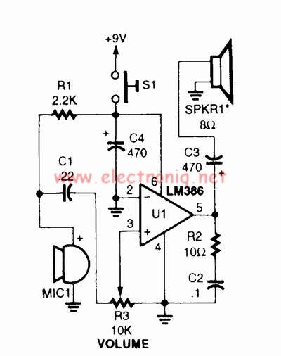
A voice amplifier can be designed using the LM386 power amplifier, which is intended for low voltage consumer applications. This simple circuit features variable gain and volume control. The gain is set internally to 20 to minimize the number...
The following circuit illustrates a power supply for an amplifier circuit diagram. Features include ease of construction and adequate electrical response. The power supply circuit for an amplifier is a crucial component that ensures the amplifier operates effectively. It typically...