
Precision Triangular-Wave Generator Uses a Single IC

The circuit design for the triangular wave oscillator is centered around the MAX9000, which integrates essential components for generating the triangular waveform. The operational amplifier is configured in an integrator configuration, where the output voltage ramps up linearly in response to a constant input voltage. This linear ramp is crucial for producing the triangular wave output. The Schmitt trigger comparator introduces hysteresis, allowing for stable switching at the defined peak and valley voltages of the triangular waveform.
The selection of resistors R2, R3, and R4, along with the capacitor C, is critical to achieving the desired frequency response and waveform characteristics. The choice of standard resistor values ensures availability and ease of implementation. The feedback mechanism through the hysteresis network allows for independent control of the triangular wave's amplitude, enhancing the circuit's versatility in various applications.
In practical applications, this triangular wave oscillator circuit can be employed in various electronic systems where precise waveform generation is required, such as in PWM control for motor drives or in signal processing for test equipment. The design's flexibility in adjusting the output voltage range and frequency makes it suitable for a wide range of engineering applications.This application note outlines the implementation of a single-supply, triangular wave oscillator using the MAX9000 and some passive components. The application circuit uses an op amp, comparator, and a voltage reference as active building blocks.
The MAX9000 is chosen because it integrates these three components. The linearity of triangul ar waveforms makes triangular wave generators useful in many "sweep" circuits and test equipment. For example, switched-mode power supplies and induction motor-control circuits often use a triangular wave oscillator as part of the pulse width modulator ( PWM ) circuit. This article presents a compact, triangular wave oscillator using a single MAX9000 IC and some passive components.
The MAX9000 device family integrates a high-speed operational amplifier, a high-speed comparator, and a precision bandgap reference. Figure 1 shows a basic triangular wave generator circuit. It is comprised of two basic building blocks: an integrator to generate the triangular wave output, and a comparator with external hysteresis (Schmitt trigger) to set the amplitude of the triangular wave as desired.
The op amp is configured as an integrator to provide the triangular output. This approach is based on the simple fact that integration of a constant voltage results in a linear ramp. The integrator`s output is fed back to its inverting input by a Schmitt trigger. The input threshold voltages of the Schmitt trigger are designed to change state corresponding to the desired peak voltages of the triangular wave output.
There is a drawback to the circuit in Figure 1: the peaks of the triangular wave can only be symmetrical about the reference voltage applied to the comparator`s inverting input. To generate a triangular wave from 0. 5V to 4. 5V, for example, a reference voltage of (0. 5V + 4. 5V)/2 = 2. 5V is needed. Since a standard bandgap reference has an output voltage of 1. 23V, it would be preferable if the voltage range of the triangular wave could be set independent of the bandgap reference.
This flexibility is achieved by adding resistor R3 to the hysteresis network, as illustrated in Figure 2 where the circuit uses the MAX9000. Resistor R3 enables the peaks of the triangular wave to be set independent of the reference voltage. The input bias current at CIN+ of the comparator is less than 80nA. To minimize errors caused by the input bias current, the current through R2 should be at least 8 µA. Current through R2 is (VREF - VOUT)/R2. Considering the two possible output states to solve for R2, two formulas result: Use the smaller of the two resulting resistor values.
For example, with VDD = 5V, VREF = 1. 23V, and IR2 = 8 µA, the two values of R2 are 471. 25k © and 153. 75k ©. Therefore, for R2 choose the standard value of 154k ©. During the rising ramp of the triangular wave, the comparator`s output is tripped low (VSS). Similarly, the falling ramp requires the comparator`s output to be at logic high (VDD). That is, the comparator must change state corresponding to the required peak and valley points of the triangular wave. Applying nodal analysis at the noninverting input of the comparator and solving for these two thresholds, gives the following simultaneous equations: In this example, the voltage range of the triangular wave is from 0.
5V to 4. 5V. Hence substituting VIH = 4. 5V, VIL = 0. 5V, VDD = 5V, and VREF = 1. 23V yields R1 = 124k © and R3 = 66. 5k ©. The maximum input bias current of the op amp is 2nA. Therefore, to minimize errors the current through R4 must always be greater than 0. 2 µA. This constraint implies that: For this example, choose f = 25kHz, VOUT, P-P = 4V (for a 0. 5V to 4. 5V triangular wave), and VREF = 1. 23V. This gives the time constant as R4 G— C = 9. 27 µs. Select C = 220pF and R4 = 42. 2k ©. The resulting output will match the designed frequency, if the op amp is not slew limited. Since the feedback capacitor ch 🔗 External reference
Related Circuits
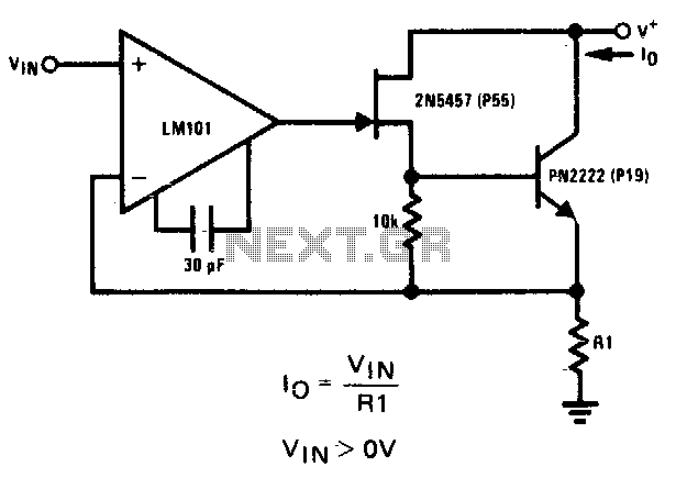
The 2N5457 JFET and PN2222 bipolar transistor exhibit high output impedance. Employing Rl as a current sensing resistor to feedback into the LM101 operational amplifier yields significant loop gain for negative feedback, thereby improving the circuit's capability as a...
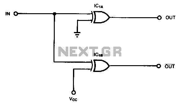
Some applications, such as driving three-state buffers for data multiplexers or for biphase clocks in high-speed systems, require complementary signals with minimal time skew and nearly simultaneous transitions. In this context, XOR gates serve as both inverting and non-inverting...
Multi Tone Alarm Description This is a simple and easy-to-build multi-tone alarm circuit that can be used in burglar alarms or sirens. The circuit is based on the dual op-amp MC1458 and LM380. The two op-amps inside the MC1458...
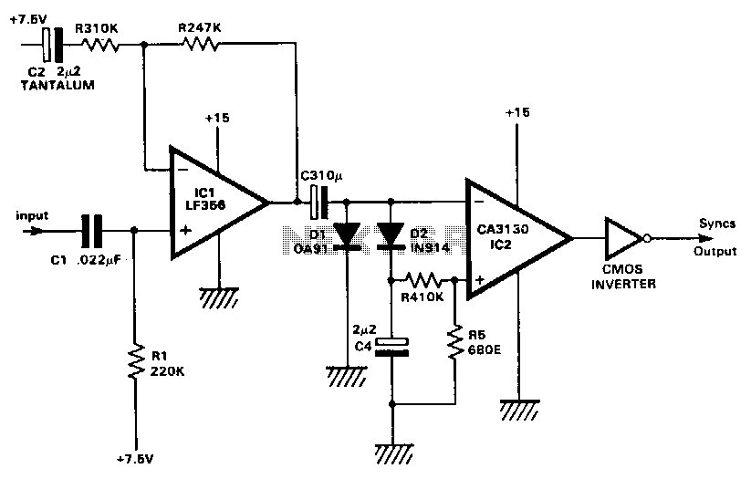
This circuit extracts the synchronization pulses from a video signal across a wide range of amplitudes and operates on a single +15 V supply. IC1 buffers and amplifies the incoming signal and applies it via C3 to the peak...
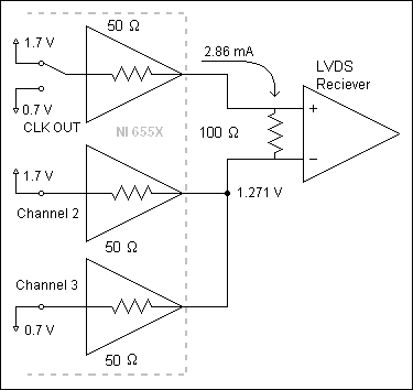
The NI 655X is a versatile high-speed digital product capable of interfacing with various technologies. This application note illustrates how to connect the NI 655X to Low Voltage Differential Signaling (LVDS) devices. LVDS is an emerging differential digital standard...
The circuit features almost open collector outputs with a withstand voltage of 60V and a continuous conduction current of 0.3A. The typical voltage drop is 0.4V, with a peak current capability of 9A. It can directly drive two windings...